This thread has been locked.

If you have a related question, please click the "Ask a related question" button in the top right corner. The newly created question will be automatically linked to this question.

BQ76952: Protection architecture on stack up and high current BQ76952

Part Number: BQ76952
Other Parts Discussed in Thread: BQ76942

Tool/software:

Dear TI team,
 
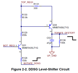
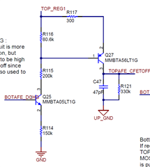
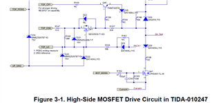
We are going to design a BMS with your BQ76952 and BQ76942 AFE. The reason why we stack up that because we need to configure the battery pack around 20-24 S. To be honest, we're still confused how to chosee the protection architecture, such as low side or high side. The battery pack should continues discharge at 150A and charge in at half of that. Could you give us some reccomendation and key aspects about this ?

Thank you for your attention to this matter. We are eager to collaborate with your team to find a solution. We await your response.

  • Hello Fairuz,

    This device is built with integrated high-side FET drivers; however, our device can also be configured to drive low-side FETs as well.

    We have some resources here that may help with your decision:

    1. Design Considerations of Stacked BQ769x2 with High-Side N-MOSFETs
      1. TIDA-010247 Reference Design
    2. How to Stack Battery Monitors for High-Cell-Count Industrial Applications
    3. Using Low-Side FETs with the BQ769x2 Battery Monitor Family

    Best Regards,
    Alexis

    1. Thanks, we've read some your reference designs and application notes. So, we've decided to apply high side protection. I got tons of question about your discrete circuit on DSG, and CHG. I read a  Design Considerations of Stacked BQ769x2 With High-Side N-MOSFET. Whereas, I still confuse how they logic works. Could you explain more about that? Such as:

      1. that reference design has a separate ground, what's voltage on TOP_REG1 and BOT REG1?

      2. I got confusing to see that circuit lol, could you explain it clearly?
      3. On the "BQ769x2 Frequently Asked Questions" document, it said "high side applications, the CHG and DSG pins voltages are the voltage of the attached battery pack plus the voltage provided by the charge pump." I'm going to separate half the battery pack so 32V each stackup. So, do each AFE CHG and DSG produce around 41V? (I'm going to configure at Settings:FET:Chg Pump Control[LVEN] 11V)

      I hope you can understand about all issues haha. Thanks a lot buddy, I'm going to wait for your response.

    2. Hello Fairuz,

      1. that reference design has a separate ground, what's voltage on TOP_REG1 and BOT REG1?

      REG1 voltage should be 3.3V for both the TOP_REG1 and the BOT REG1. This can be found in Section 2.1 Data Communications of the Design Considerations of Stacked application note.

      2. I got confusing to see that circuit lol, could you explain it clearly?

      Which part of the circuit are you asking for more clarity on?
      Section 3.1 Discharge MOSFET Turn ON and Off Processes and the following sections, go over the circuit more in detail to help explain the design.  

      3. On the "BQ769x2 Frequently Asked Questions" document, it said "high side applications, the CHG and DSG pins voltages are the voltage of the attached battery pack plus the voltage provided by the charge pump." I'm going to separate half the battery pack so 32V each stackup. So, do each AFE CHG and DSG produce around 41V? (I'm going to configure at Settings:FET:Chg Pump Control[LVEN] 11V)

      If you configure the charge pump to be 11V, then you can expect the CHG and DSG pins to be around the voltage of the attached battery pack + 11V.

      Best Regards,
      Alexis

    3. Ok thanks a lot