


Tool/software:
Previously, I mentioned in this thread that I was obtaining incorrect positive voltage values and that there were some noisy sounds in the circuitry:
I realized that the solder paste I was using had some issues, and no matter how much I cleaned it, there was still some conductivity. I redesigned the circuit by increasing it to four layers and soldering the components manually without using solder paste, which allowed me to obtain the correct values.
I am sharing this circuit below as a reference in case someone encounters a similar issue.


However, I need to design this circuit as a two-layer board. I converted the successful four-layer design into a two-layer one without changing the component positions.
I am sharing the relevant images below:


In this design, the +22V, -20V, -15V, and VCOM values are as expected. However, while the VPOS value is stable, it remains at 16V instead of 15V.
In my tests, I obtained the same result using the other same chips and boards, so I believe this issue is related to the design. Therefore, I am working on a new design.
By reviewing previous posts, I am making the following improvements:
1. Reducing the loop length
2. Placing capacitors as close to the pins as possible
3. Avoiding any traces running beneath the VPOS-related area
4. Isolating the VPOS-related area using vias
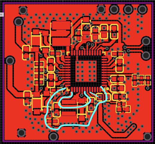
I am sharing the latest images of the circuit and the Gerber file below:


Gerber_TPS65185_module_TPS65185_2_LAYER_2025-03-04.zip
At this stage, could you review the design and suggest any possible improvements? If you notice any errors, please point them out.
I have mainly focused on the marked area, assuming it is related to VPOS. However, do other areas have any impact on this value?
It would be best to finalize the design based on your advice before placing the order.
thank you
