


Other Parts Discussed in Thread: BQSTUDIO
Tool/software:
hi.
I am controlling the BQ34Z100-R2 using a uC on a self-made PCB.
Currently, data can be read and written to Data Flash.
What I'm wondering is what the BQ34Z100-R2 TRM says and what I actually read when I read the data is different.

The above content is the content of Data SUBCLASS of Configuration CLASS of Data Flash provided by TRM.

Figure 1
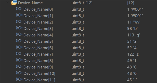
Figure 2
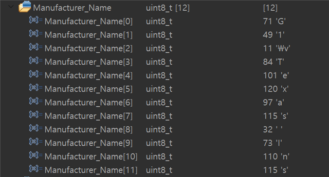
Figure 3
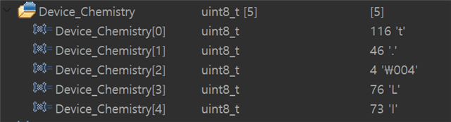
Figure 4
The above is the data actually read from BQ34Z100-R2.
When I compare the TRM of BQ34Z100-R2 with the data I read, the data matches up to OFFSET 30.
(Except that the Design Energy value of OFFSET 13 is read as 370 -> 5400 and the JEITA T1 value of OFFSET 26 is read as -10 -> 0.)
You can see that 3 bytes have been pushed back from OFFSET 31.
I understand that the value of Device_Name[2] in Figure 1, 11, represents the size of bytes used for Device_Name. Is that correct?
So, does that mean that the values of OFFSET 31 and 32 become the values of Volt Scale and Curr Scale respectively?
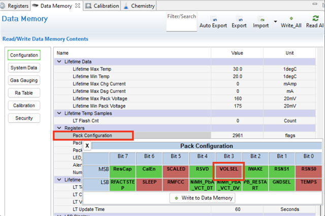
And the figure below is the Pack Configuration Register Bits table provided by TRM.

In this table, Bit 5 of the High Byte is marked as Reserved.
The image above is taken from the TI forum.
In this figure, you can see that Bit 5 of the High Byte is SCALED. This is different from the TRM.
The TRM version I'm looking at is Revision A. Has there been any update since then?
