Tool/software:
Hello everyone,
We are testing an ORing circuit using the LM73100 ideal diode controller and are encountering an unexpected voltage dip of approximately 2-3V for 6ms. I would appreciate any insights on this issue.
Circuit Setup:
- Load Current (Considering RIstart as 6ohm): 2A ( Maximum load of 5A and continuous load of 3A)
- Input Voltages: Primary Power Supply = 12V, Secondary Power Supply = 12V
- Output Capacitance: 470µF
- Cdvdt: 1.8nF
- DSO Probe Color Mapping:
- Green: 12V_ORing (output)
- Blue: Secondary Power Supply
- Yellow: Primary Power Supply
Test Scenarios & Results:
Test 1 (Ideal Condition - DSO Image 1: oring_01.png)
- Initial State: First Primary Power Supply is turned ON, then Secondary Power Supply is turned ON
- Transition Trigger: Primary Power Supply turned OFF
- Observation: Power switching works as expected although there is voltage dip of approximately 2-3V

Test 2 (Failure Case - DSO Image 2: oring_02.png)
- Initial State: First Secondary Power Supply is turned ON, then Primary Power Supply is turned ON
- Transition Trigger: Primary Power Supply turned OFF
- Observation: The ORing output fails and the output of ORing is turned off completely

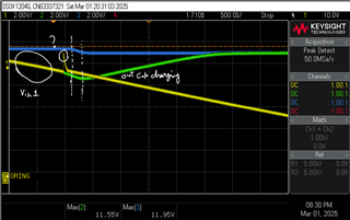
Test 3 (Simultaneous Startup - DSO Image 3: oring_03.png)
- Initial State: Both supplies turned ON at the same time
- Observation: The ORing output gradually ramps up, showing how the circuit behaves during a cold start when both supplies are activated simultaneously.

- A wider view of Test 3, showing the ORing behavior over a longer timespan.

Issue:
According to calculations, the slew rate should be sufficient, but during actual testing, we see an approximate 2-3V voltage droop in certain cases. This could potentially impact system stability at higher loads (target 5A).
Request for Help:
- Is this voltage dip expected given the component values?
- Could there be an issue with Cdvdt selection or output capacitance?
- Any suggestions to mitigate the voltage dip and ensure a smooth transition?
- Why does the ORing output fail in Test 2?
- Is there any internal fault latch that is being triggered which leads to failure in Test 2?
Attached are DSO images and data files for reference. Looking forward to your opinions!
Thanks in advance! and kindly let me know if any additional information is needed from my end.