This thread has been locked.

If you have a related question, please click the "Ask a related question" button in the top right corner. The newly created question will be automatically linked to this question.

UCC3818A: Bais Resistor Caculate

Part Number: UCC3818A
Other Parts Discussed in Thread: UCC3818

Tool/software:

Hi 

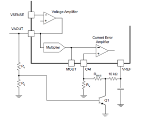
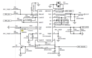
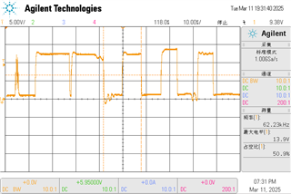
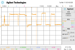
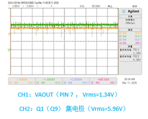
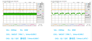
For last UCC3818A noise issue, this problem is still. and now we want to check the CAI pin. and  we read application note slua309c. but we don't know how to caculate the Rbias in slua309c as below picture 1. also the R61 (highlight as orange) in picture 2 ( customer schematic) . Could you help tell us how to caculate it ? or provide relate caculate file. It's best if you can help caculate it. thanks.

  920W_SCH.pdf

  • Hello Jonas, 

    Actually the SLUA309C app-note does describe how to determine Rbias value, but it is rather obscure.  There is no dedicated calculator file for this. 

    The basic solution is to add a positive offset voltage to the (+) input of the CA (CAI pin).  The question is how much offset voltage?

    The app-note text refers to the maximum offset voltage of the CA inputs, which the datasheet indicates is +2.5mV / -3.5mV.    The worst case is -3.5mV across your Rx resistor of 3.6kR.  3.5mV/3.6k = -0.97uA

    The app-note text refers to the maximum zero-current output of the multiplier, which the datasheet indicates is -3.5uA over full temperature range.  Adding the -0.97uA from the CA offset voltage to the multiplier "zero current" = -3.5uA + -0.97uA = -4.47uA = ~-4.5uA. 

    So at least +4.5uA is needed from VREF to bias CAI up positive high enough to cancel the influence of the -4.5uA offset current.  
    Rbias = VREF/4.5uA = 7.5V/4.5uA = 1.67MR.  

    I suggest to apply a little margin and use 1.50MR, but too much lower will have too much offset and this will increase THDi. 

    Regards,
    Ulrich

  • Hi Ulrich:

    Thanks for your feedback. and other question, customer use R60:1K ,R63;100K  R64:470K,could you help check those value is ok or not ? could you help suggest those resistors's value ? thanks

  • Hello Jonas, 

    Page 3 of the SLUA309C app-note also describes how to determine R1 and R2 (R63, R64) values in principle, but again, I think the details are rather obscure.  I think a numerical example would have been helpful. 

    1.  First, 1kR for R60 is too low.  When Q1 is on, it will pull 7.5V/1kR = 7.5mA from VREF, and VREF is characterized at only ~2mA loading:

    I recommend to change R60 to 100kR (yes, 100kR, not 10kR as in the app-note), so VREF load is </= 75uA. 

    2.  Next, Q1 should be off when VAOUT = 1V, but on when VAOUT rises higher.  Using MMBT4401L datasheet (I could not get a clear Leshan DS), Figures 14 and 15 indicate that Q1 would be saturated with a beta of 10, which is 7.5uA.  But we want ~0uA base current when VAOUT = 1V.  
    Figure 18 shows that we want Vbe to be < 0.5V at 25C or even lower at higher ambient temperatures.  

    For your case, I estimate 0.4V will be low enough to keep Q1 off, so 0.4V/470kR (R64) = .85uA.  This current must flow through R63 when VAOUT = 1V, so R63 = (1-0.4)/0.85uA = 705kR.  Choose R63 = 750kR to lower Vbe a little at VAOUT = 1V (for margin).

    3.  Next, Q1 should turn on when VAOUT > 2V.  To saturate Q1, Ib =Ic/10 = 7.5uA.  Collector current from Rbias will be negligible. 
    Figure 17 indicates that Vbe will be around 0.5~0.6V in this condition.  Using 0.55V for calculations, Ib + I_R64 = I_R63.  7.5uA + 0.55V/470kR = 8.67uA.  (2V -0.55V)/8.67uA = 167kR for R63.  But R63 will be a load on VAOUT at full PFC output power. 
    I suggest to set R63 = 220kR.  At max-load, VAOUT = ~5.5V.   (5.5V - 0.6Vbe)/220kR = 22uA load on VAOUT at max load.  This seems to be a reasonably small portion of the 150uA sourcing capability of VAOUT.

    Since these calculations involve some approximations and estimates of small voltages at small currents, and since the Vbe of Q1 will vary with ambient temperature and current, I recommend to install the calculated resistor values and the evaluate the performance of the offset circuit over temperature. 
    Adjust the values of R63 and R64 to optimize the load level where the CAI offset is removed.  Probably adjusting R63 will be enough. 

    Regards,
    Ulrich

  • Hi

    1. Which parameter difference in bad IC causes OVP in PFC under extremely light load conditions? When the PFC exits the OVP state, why does the bad IC adjust the duty cycle of the driving waveform to the maximum? What causes the noise caused by the PFC inductor under extremely light load conditions?
    2. Can the differences in this parameter be screened or intercepted during original production testing?
    3. Will this chip that causes noise in PFC inductors lead to chip failure or reduced reliability during long-term use? Will it cause PFC line device failure?
    4. Have this IC changed in the past five years (for example: origin, wafer, process, packaging and testing, line design, etc.)?
    5. The SLUA309C document describes that OVP will enter under light load. Does the PFC voltage (i.e. the voltage on the BULK capacitor) exceed the set overvoltage protection point? Does the UCC3818 enter overvoltage protection (i.e. the PIN10 protection)? However, when the poor IC is no longer loaded, the PFC voltage has no overvoltage (CH2 green in the waveform shown in the figure below). Please explain why the chip has OVP protection and hiccups? Why is the duty cycle of the driving waveform adjusted to a large extent when hiccups are restored? The maximum measured reaches more than 90% (CH1 in the figure below).

  • Hi 

    The following are the actual test results after modification based on TI's resistance parameters.
    1. TI calculation R61 must be changed to 1.5M. In actual tests R60=1K, R61=1.5M, R63=100K, R64=470K can solve the problem of noise in PFC inductor (the following waveform), but at 10% load (Po=100W), the harmonic cannot pass through CLASS D.

    2. Actual tests R60=1K, R61=2.3M, R63=100K, R64=470K can solve the problem of noise in PFC inductance caused by bad chips. The harmonics can also pass through CLASS D, but the resistance value of R61 is less than the calculated value of TI (1.67M).

    3. TI calculates R60=100K; R61=1.5M, R63=220K. In actual tests, R60=100K, R61=1.5M, R63=220K, R64=470K, VAOUT (PIN 7) voltage is stable, but Q1 (Q9) has oscillation, iTHD is very large, and the value is unstable.

    So what value for those resistor could slove this issue ? thanks

  • Hello Jonas, 

    I need some time to analyze your latest information, but I will be out of office tomorrow, so i won't be able to work on this until next week. 

    Please allow me this time.  

    Regards,
    Ulrich

  • Hello Jonas, 

    2. Actual tests R60=1K, R61=2.3M, R63=100K, R64=470K can solve the problem of noise in PFC inductance caused by bad chips. The harmonics can also pass through CLASS D, but the resistance value of R61 is less than the calculated value of TI (1.67M).

    Based on your statement #2, it looks like you have found a solution.  
    Even though your resistor values are not the same as what I calculated, if it works in your application, I suggest to use it. 

    Regards,
    Ulrich