This thread has been locked.

If you have a related question, please click the "Ask a related question" button in the top right corner. The newly created question will be automatically linked to this question.

UCC28051: How to utilize Zero Power Detect block for Flyback PFC Applications

Part Number: UCC28051
Other Parts Discussed in Thread: UCC28810,

Tool/software:

Hello,

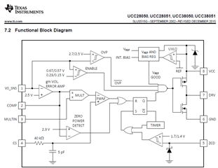
I am referring the design document for the 48W ceiling fan (), which uses UCC28810. The internal block diagram for both the ICs is the same.

UCC28051 internal block diagram:

UCC28810 internal block diagram:

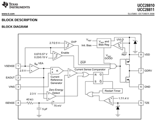
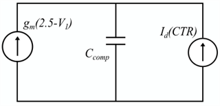
For the application note attached, where UCC28810 IC is used in a flyback topology with output voltage sensed through an auxiliary winding and opto-coupler, fed to pin 1 and pin 2, respectively. How does the zero power detect block (connected to the comp pin IC) get activated during output light load/no-load conditions?

P.S.: I know the pin 3 voltage has to drop below the comparator ref voltage (2.3V for the zero power detect case). What I am asking is, during light loading, how is that voltage with the below circuitry reflected on the pin 3 cap?

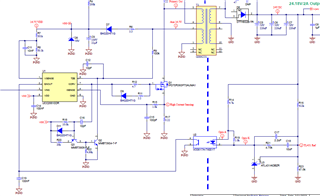
48W Ceiling Fan TI ref design.pdf

Thanks,

Shivam Chakraborty

  • Shivam,

    I assume you mean the voltage on the pin 2 cap, not pin 3. during light load condition, the feedback look will drive the opto-coupler to pull more current from EAOUT pin and eventually drag down its voltage below 2.3V (the Gm amplifier sourcing capability is 10uA only when OVP is not triggered). Then the AND gate after the zero energy detect block will latch PWM low, preventing further energy transfer to the secondary side. As long as there is a load, Vout will drop without energy transferred from the primary side. Then the EAOUT voltage will increase and the latch will be released.

    Hope this clarifies.

    Ning

  • Hi Ning,

    Yes, I was talking about the pin-2 cap. Sorry for the typing error !

    Thanks for the explanation; now I am a bit clear. I wanted to understand the behaviour of the cap placed on pin 2. Is the analysis (as shown in the image below) of the pin 2 cap behavior correct?

    Where,

    gm is the transconductance of the error amplifier (90 uS) per the datasheet.

    2.5V is the internal reference to the error amplifier connected on pin 1.

    Id is the opto-coupler diode current connected on the secondary side.

    CTR is the current transfer ratio of the optocoupler connected on the secondary side.

    Sorry! if the answer to the question is kinda obvious. I am having difficulty understanding the behavior of the cap connected to pin 2. Also any document to understand/model the control loop of flyback with opto-coupler on secondary would be helpful. 

    Thanks and regards,

    Shivam

  • What is V1 in your drawing? The Id direction should be opposite in your drawing.

    Here are few files you can read for loop design.

    https://www.ti.com/lit/an/sluaa66/sluaa66.pdf

    https://www.ti.com/lit/an/slla618/slla618.pdf

    There are many YouTube videos you can watch to learn this topic.

  • V1 refers to the pin 1 voltage of the IC (V0_SNS). Yes, you are correct. The direction should be the opposite.

  • Keep in mind that the max current of the amplifier is 10uA under normal operation condition.