This thread has been locked.

If you have a related question, please click the "Ask a related question" button in the top right corner. The newly created question will be automatically linked to this question.

TPS54320: external clock should be AC or DC coupled to RT/CLK pin?

Genius 3900 points
Part Number: TPS54320

Tool/software:

hi there,

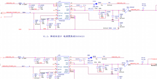
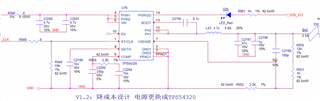
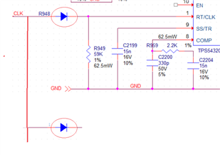
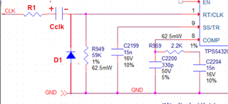
we have 3 TPS54320 on board. sch as below. FPGA IO provides external clock to drive both three power IC. 800khz

At the beginning, FPGA output  external clock as as HIGH signal, we hope the IC works by RT resistor. however, at this time, the PH waveform is about 60khz, and the output ripple is large as 1Vpp. this is abnormal.

then FPGA output 800KHZ 50% duty cycle external clock, and after 50ms, the PH waveform is ok 800khz.

And evern very strange, this problem happens occasionally when the temperature is -20°C on different boards.  we can repeat this phenomena by use freezer spray on TPS54320.

We noticed that 3 RT resistor are actually in parallel, so the equivalent RT resistor is 59K/3. but we can not understand how the 60khz PH come from.  Questions:

1, could you pls provide the internal structure of RT/CLk pin inside thee IC? 

2, we tried change the 0 ohm on external clock (R948, etc)  to a Capacitor, and things become normal when ac coupled. We do not want to insert 3 independent buffer (PCB revision), can we use like this? there is no relevant info in datasheet.

any other advice is welcome, especially about the low temperature.

  • Hi,

    For single chip, the RT pin has fixed voltage Vref, the source current =Vref/RT will determine the switching freq. 

    If you bias the high voltage >Vref on RT pin, then the source current is zero and device working on lowest freq.

    if you simply parallel 3 RT pins together, then each device RT pin will only source 1/3 current if their Vref is same.

    Below some solution:

    1. Use small Schottky diode instead of 0 ohm resistor to isolate each RT pin

    2. set FPGA Clock I/O is high impedance or low level before sending out clock

    If cap is used instead of 0 ohm, then you need to add Schottky diode parallel with RT resistor to protect the reverse voltage when clock is low.

  • hi Andy, thanks for replying

    1, can you explain how to connect the schottky diode to isolate each RT pin? 

    2, we can try this. but if set FPGA I/O Low, the votage on RT pin will be 0V, will this be ok?

    3, how to connect the parallel diode? why there is Reverse Voltage 

    Thanks

  • Isolated by Schottky diode:

    If FPGA I/O keeps low, each converter will works at freq set by RT pin, 

    No requirement on I/O status if Isolated by cap 

    But the cap block the DC voltage of clock, so RT pin will see negative voltage if no clamp diode on RT pin.

    and it's better to add R1 round 1K to limit the reverse current.

  • Hi Andy, thanks for answering.

    By the way, do you have any suggestion about this phenomenon " very strange, this problem ONLY  happens occasionally when the temperature is around -20°C on different boards.  we can repeat this phenomena by use freezer spray on TPS54320." Thanks!

  • Hi

    Pls re-test at low temp with the circuit I suggested, the problem you met maybe caused by improper RT connection

  • Hi,Andy

    We will test your solutions later. 

    We tried another method. we adjust the timing sequence as below : 

    FPGA provide external 800K CLK at first, wait for 3s, then enable IOBOARD_12V ( the upstream DC/DC  ) . it seems working fine at low temp. 

    will this working conditions damage 54320 ?