This thread has been locked.

If you have a related question, please click the "Ask a related question" button in the top right corner. The newly created question will be automatically linked to this question.

LM5160-Q1: SW output waveform

Part Number: LM5160-Q1
Other Parts Discussed in Thread: LM5160

Tool/software:

Hi,

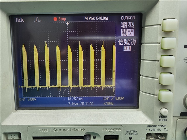
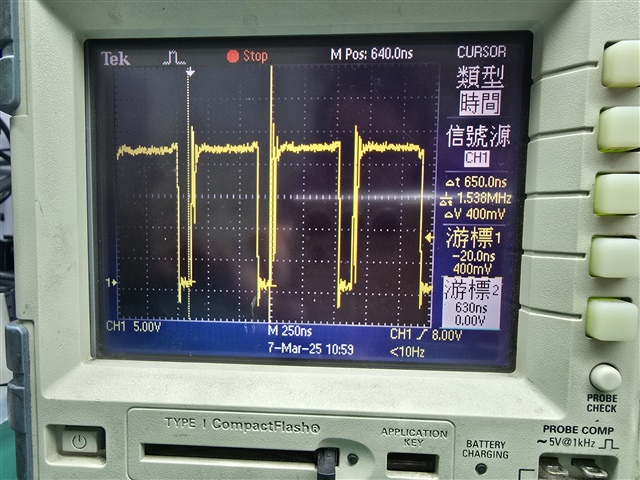
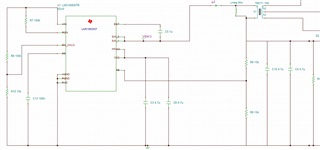
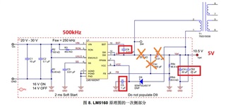
I designed a circuit using LM5160, with an input voltage of 20V, an output voltage of 5V, and a Ron of 100k, so the switching frequency is 500kHz. However, the SW waveform I measured is very strange. Can you tell me what the problem is?

  • Hi Lin,

    Can you please share your schematic or the filled excel tool LM5160DNTBK-CALC Calculation tool | TI.com with your operating conditions?  What are the values of ripple injection network components?  Sufficient ripple is required at FB node for proper and stable switching. Also, what is the operating load current?

    Regards

    Arpita

  • Hi Aprita,

    What would happen if I didn't use R3?

  • Hi Lin,

    Note that you must use proper R3 in series with output capacitor to have sufficient ripple magnitude at feedback node(as you don't have Type 2 or Type-3 injection circuit). You can calculate the minimum required value of R3 from device datasheet. as shown below.


    Type 1 ripple circuits couple the ripple from the output of the converter to the feedback node (FB). The output voltage ripple has two components

    1. Capacitive ripple:  caused by Cout ( the inductor ripple current charging or discharging the output capacitor.)

    2. Resistive ripple: caused by R3 and ESR (the inductor ripple current flowing through the ESR of the output capacitor and R3.)

    For proper operation of the device and stable switching, the resistive ripple must exceed the capacitive ripple at output (VOUT). If you don't use the minimum required R3, the above condition won't be satisfied. As a result, unstable switching behavior is observed in COT converters with multiple on-time bursts in close succession followed by a long off-time. 

    Please try connecting proper R3 in series with Cout and capture the SW waveforms. This should resolve the issue.

    For more information. please refer to the https://www.ti.com/lit/an/snva166a/snva166a.pdf?ts=1741326202372.

    regards

    Arpita

  • Hi Aprota,

    Thanks.

    If the primary load of my design is very small, do I need to add a dummy load? If so, how much is recommended?

    Or only need to design Resr and not add anything else?

  • Hi Aprota,

    I reworked my circuit, I added a 1 ohm resistor, but the waveform looks similar.

    Resr > 25m * Vo / Vref / △IL

    Vo = 5V,Vref = 2V , △IL=0.3

    Resr = 25 m * 5 / 2 / 0.3 =  0.208

  • Hi Lin,

    Please share the schematic detailed review and further debugging. 

    Regards

    Arpita

  • Hi Aprita,

    Please see the following picture.

    I added a Resr at the output cap,the wavwform is the same.

    The same is true with a smaller Cbst.

    Ron is 100k,it's ok.

  • Hi Lin,

    From schematic I can see you are using fly-buck configuration. You have not mentioned about isolated output voltage.

    Could you please share the complete schematic and filled calculator for fly-buck calculator FLYBUCK-FLYBACK-DESIGN-CALC Calculation tool | TI.com  for the operating conditions and share with us for further debug. Let us know the load current on both primary and secondary sides. Could you please capture waveforms of non-isolated and isolated output voltages?

    Some preliminary comments on the partial schematic: Recommended values for C_VCC and CBST are 1 µF and 10 nF, respectively. Current values are pretty high. Please follow the recommended values for reliable operation.

    Regards

    Arpita

  • Hi Aprita,

    The design is based on this document.

    https://www.ti.com.cn/cn/lit/ug/zhcu106a/zhcu106a.pdf

    I add Resr at the output cap,but it's similar.

    Ipri is almost 100mA,The secondary side load is about 1W, but it is not loaded yet.

  • Hi Aprita,

    I changed C_VCC and CBST to 1 µF and 10 nF.

    Add a Resr at Cout is 5 ohm.

    The wave form of Vsw is the same.

  • Hi Lin,

    Thanks for confirming that you are using fly-buck configuration. Please note that Type-3 ripple injection network is required for fly-buck mode of operation (refer to datasheet section 8.2.2.2.3) 

    Your schematic and operating conditions look different from the example. You need to fill in calculator https://www.ti.com/tool/download/FLYBUCK-FLYBACK-DESIGN-CALC. The excel will guide to choose Type-3 ripple network for Fly buck operation. Also, please double check the RON value for 500kHZ using the calculator. Present value seems smaller. You should always follow the recommended values of components. Using random values of components may lead to improper behavior of the device or damage. 

  • Closing the thread due to inacitivity.

    Regards

    Arpita