This thread has been locked.

If you have a related question, please click the "Ask a related question" button in the top right corner. The newly created question will be automatically linked to this question.

TPS25751: Sink PDO configuration without EEPROM.

Part Number: TPS25751

Tool/software:

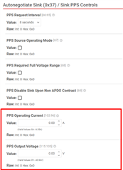
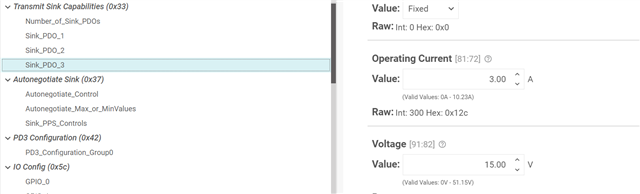
Hi, we are using the TPS25751EVM and we want to change the PPSOutputVoltage to 15V but we do not want to use the customization tool or any other application, We want to change the value with I2C, and when we are trying to write the configuration to the TX_SINK_CAPABILITIES register the PPSOutputVoltage is not getting changed and the values read from the register remains same (according to the customization tool configuration).
Will the output value be changed only when the EEPROM is not connected? Asking this query as we are planning to use the TPS25751 IC and the only communication present will be I2C.

  • Hi Runita, 

    Thank you for reaching out!

    See below for steps on how to configure PPS Sink: 

    1- Configure Transmit Sink Capabilities Sink PDO:

    • Supply Type: Sink PPS
    • Maximum Current in PPS contract.
    • Minimum Voltage in PPS contract.
    • Maximum Voltage in PPS Contract.

    2- Configure ‘Sink PPS Controls’ section of ‘Autonegotiate Sink Register’ (0x37)

    • Toggle PPS Enable Sink Mode [64] to enable PPS Sink
    • Configure desired initial PPS operating current and output voltage

    3- MCU will need to update the PPS Operating Current and PPS Output Voltage when new Request message is desired

    See Section 5.4 in the TRM for more details. 

    Best Regards, 

    Aya Khedr

  • Hi Aya,
    We cannot use the application to configure the IC as per our requirement so we want to know the process to set the PDO value to 3 and set the output voltage as 15V with 3A current in the TX_SINK_CAPABILITIES register.

    Please refer to following image to see the values we need to update but without the customization tool.

    I tried to directly write the value the TX_SINK_CAPABILITIES register with the values defined in the application but the values are not getting updated in the register. I checked it with and with the EEPROM connected.

  • Hi Runita, 

    See clarification below on how to configure the TPS25751. 

    An EEPROM is not required to use the TPS25751. However, if you do not want to use an EEPROM, you will need an MCU to load the configuration in place of the EEPROM.

    From the datasheet:

    "8.4.1 Pin Strapping to Configure Default Behavior

    During the boot procedure, the device reads the ADCINx pins and set the configurations based on the table below. The device then attempts to load a configuration from an external EEPROM on the I2Cc bus. If no EEPROM is detected, then the device waits for an external host to load a configuration"

    To use an MCU to load your configuration, you would use 4CC commands over I2C. Section 4.4 of the Technical Reference Manual details these commands. Section 5 details the flow for Patch Burst Mode (PBM), which is the name for this process. A low region binary file, generated from the USBC PD Application Customization Tool would be loaded onto the PD controller during PBM. 

    Please let me know if you have additional questions.

    Best Regards, 

    Aya Khedr

  • Hi Aya,
    I am following the instructions you refered to from the TRM, I have connected the VIN_3V3 and the IRQ_t pin of the EVM to my MCU and the EEPROM is disconnected so the USB-PD controller is in "PTCH" mode. Now the second step is to read the INT_EVENT register, which is read empty. Can you tell me the reason for this? 

    I also have another query, I wanted to know what is the default output voltage for the IC when the configuration is not set yet?

  • Hi Runita, 

    Could you share a block diagram of your connections so that I can fully understand your setup? Do you have the I2Ct_SDA and I2Ct_SCL pins connected to your MCU as well? 

    What is the ADCIN configuration set to on the EVM? How is the EVM being powered?

    Best Regards, 

    Aya Khedr

  • Hi Aya,

     We cannot share the block diagram with you but I can explain the connections to you. The I2Ct pins are connected to our MCU,  and the ADCIN configuration is:
    ADCIN1- 7, ADCIN2- 5.

    The EVM is getting the power through J3 connector connected to a 65W power supply with C type connection pin.

    Can you clarify me that if I want to read the interrupt events specified in the register like if the plug is connected or not what is the procedure from the FW? and the pin configuration (I2Ct_SCL, I2Ct_SDA, and IRQt pin) with the USB-PD controller and MCU along with any power specifications.

  • Please see the below process to read the INT EVENT reg for the Patch bundle ready interrupt on the 81st bit of the register:

    in the first step the mask is set for the interrupt in the INT MASK reg(0x16), then the bit written is confirmed by reading the mask register and then the interrupt event is read but the register is still read empty.

    reVal = LPI2C_read_reg(I2C0_MASTER, INT_EVENT_REG_ADDR, USB_PD_CONTROLLER_SLAVE_ADDR, int_mask_buffer);

    int_mask_buffer[11] |= 1;

    reVal = LPI2C_write_reg(I2C0_MASTER, INT_MASK_REG_ADDR, int_mask_buffer, USB_PD_CONTROLLER_SLAVE_ADDR,

    11);

    reVal = LPI2C_read_reg(I2C0_MASTER, INT_EVENT_REG_ADDR, USB_PD_CONTROLLER_SLAVE_ADDR, int_mask_buffer);

    reVal = LPI2C_read_reg(I2C0_MASTER, INT_EVENT_REG_ADDR, USB_PD_CONTROLLER_SLAVE_ADDR, int_event_buffer);

    SysTick_DelayTicks(10U);

    reVal = LPI2C_read_reg(I2C0_MASTER, INT_EVENT_REG_ADDR, USB_PD_CONTROLLER_SLAVE_ADDR, int_event_buffer);

    I2C logs:
    Step 1: mask is set

    Step 2: interrupt event register read after the delay

    Let me know if any process is wrong or anything else needs to me changed.

    This above process is in "PTCH" mode.

    Another observation is that when I try the same process in "APP" mode this event register is set according

    to the mask properly.

  • Hi Runita, 

    I will review and get back to you with feedback early next week. 

    Best Regards, 

    Aya Khedr

  • Hi Aya,

    Do you have any update regarding this issue? We need to check if the patch file can be uploaded without EEPROM and GUI tool as soon as possible and I am still not getting the int_event_reg bit related to the device is ready to receive the patch file, I have tried to use the INT_MASK_REG to set the interrupt but this register is also being read empty without the EEPROM.

    write buffer:

    read buffer:

  • Hi Runita, 

    Please ensure that J16 is removed (EEPROM disconnected) and that I2Ct_SCL, I2Ct_SDL, I2Ct_IRQ, GND are all connected to your MCU. 

    Please let me know if you have additional questions. 

    Best Regards, 

    Aya Khedr 

  • Hi Aya,

    I am getting the INT_EVENT1 register bit as required but I am not getting the DATA1 register cleared after the "PBMs" command is sent and the CMD1 register is read '0'. 

    Please refer to the data that I am writing in the DATA1 register as referred from the TRM under the "PBMs" 4CC task description, let me know if any errors in the values that I am writing in the register or the method. 

    Note that my patch bundle size is 32768 bytes and the target address is set according to the ADCINx pin configurations.

    reVal = LPI2C_read_reg(I2C0_MASTER, DATA_REG_ADDR, USB_PD_CONTROLLER_SLAVE_ADDR, data_buffer,65);

    data_buffer[0] = 7;

    data_buffer[3] = 0x00;

    data_buffer[4] = 0x00;

    data_buffer[5] = 0x80;

    data_buffer[6] = 0x00;

    data_buffer[7] = 0x21;

    data_buffer[8] = 0x32;

    reVal = LPI2C_write_reg(I2C0_MASTER, DATA_REG_ADDR, data_buffer, USB_PD_CONTROLLER_SLAVE_ADDR,

    9);

    reVal = LPI2C_read_reg(I2C0_MASTER, COMMAND_REG_ADDR, USB_PD_CONTROLLER_SLAVE_ADDR, command_buffer,5);

    uint8_t write_command_buffer[COMMAND_REG_LENGTH] = {0x04, 0x50, 0x42, 0x4D, 0x73};

    reVal = LPI2C_write_reg(I2C0_MASTER, COMMAND_REG_ADDR, write_command_buffer, USB_PD_CONTROLLER_SLAVE_ADDR,

    5);

    reVal = LPI2C_read_reg(I2C0_MASTER, COMMAND_REG_ADDR, USB_PD_CONTROLLER_SLAVE_ADDR, command_buffer,5);

    reVal = LPI2C_read_reg(I2C0_MASTER, DATA_REG_ADDR, USB_PD_CONTROLLER_SLAVE_ADDR, data_buffer,65);

  • I am getting the output value in the DATA1 register as 5 (invalid target address), can you tell me what should be the target address in this case, I am writing 0x21 in the BYTE5 of the DATA1 register.

  • Hi Runita, 

    Please see the following Application Note that details each step of the PBM process. 

    This would be the Data1 register write. 

    Best Regards, 

    Aya Khedr

  • Hi Aya,

    Thanks for the reference, I tried to send the same data as per this application note and please check the data register buffer log to confirm if I am getting the correct response form the DATA1 register for command "PBMs".

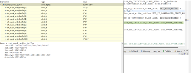
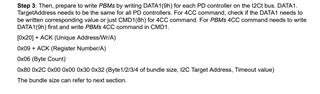
     this is the response after PBMs command

    According to my understanding the command was successful so I sent the patch bundle and then the PBMc command, But now I am getting the following value in the DATA1 register. The CMD1 register is giving the correct response according to the application note reference.

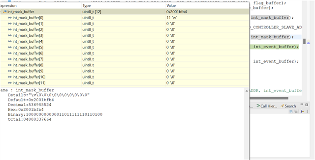
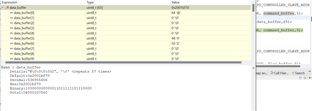
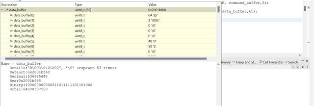
     this is the response after PBMc command.

    Note that my patch bundle transfer was successful.

  • Hi Runita, 

    Have you been able to successfully complete the PBMx process? If not, which step of the process is not successful?

    Best Regards, 

    Aya Khedr

  • Hi Aya,

    After the burst data is transferred successfully I sent the command "PBMc", the CMD1 register is cleared as per the method but the DATA1 register is not getting cleared according to the application note and the TRM, I have shared my DATA1 register value in the above message's second image. 

  • Hi Runita, 

    This seems to be a duplicate of the following thread: e2e.ti.com/.../5731631

    Could you please confirm if these are the same?

    Best Regards, 

    Aya Khedr