This thread has been locked.

If you have a related question, please click the "Ask a related question" button in the top right corner. The newly created question will be automatically linked to this question.

UCC5350: SIC gate driver design questions.

Part Number: UCC5350
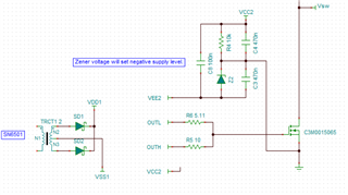
Other Parts Discussed in Thread: SN6501,

Tool/software:

Hello,

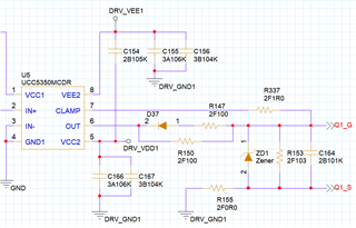
I have designed a gate drive circuit utilizing the UCC5350M.

Would there be any issues with applying a negative voltage to the VEE2 pin?
I would appreciate any technical advice or feedback on the circuit design.

The circuit is designed for use with a SiC FET.

VCC2: 18Vdc
VEE2: -3Vdc

I would be grateful for any insights or recommendations.

Best regards,

  • Hi Tae Jin Ko,

    There is no issue with using a negative voltage at VEE2 with respect to Q1_S. This is indeed a benefit to using an isolated gate driver. Since the output stage is floating with respect to the input side's voltage, you can use an isolated power supply. This can easily be shifted into a three-level supply, to generate a negative turn-off voltage, with a simple Zener diode and resistor circuit, with parallel decoupling capacitors. 


    NegativeBiasTurnoff.TSC

    My recommendation is to still put a VCC2-VEE2 capacitor closest to the UCC5350, since this will protect both the pull-up network and the pull-down network from transient overvoltage. You can use an SN6501 and a small push-pull transformer to generate an isolated supply rail for the output side.

    Best regards,

    Sean

  • Hi Sean,

    Thank you for your help!

    The issue has been successfully resolved.

    Best regards,

    Tae Jin