This thread has been locked.

If you have a related question, please click the "Ask a related question" button in the top right corner. The newly created question will be automatically linked to this question.

TPS40322EVM-679 about design procedure

Other Parts Discussed in Thread: TPS40322

Hi,

I am newbie in power supply design, so I might have some dumb questions. Please generously understand that. 

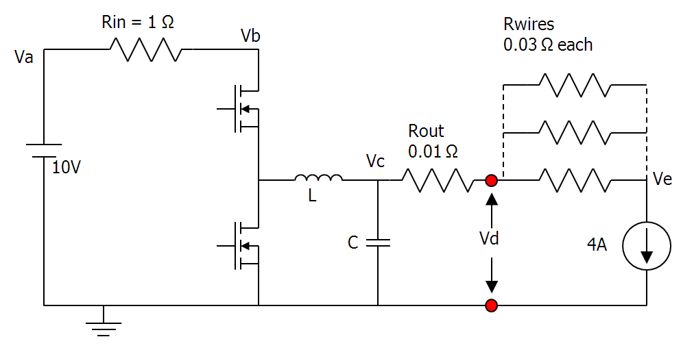
I am using TPS40322EVM-679 evaluation board to generate1.0V and 1.5V output with 12.0V input voltage.When I measured the efficiency of the board with 4A current draw from the load for 1V output, and 1A current draw from 1.5V output, I got around 84%. I am wondering if I can increase the efficiency even higher than this by decreasing Pulse Width Modulation frequency. It seems that I need to change many components if I want to change PWM freq, so I am trying to understand the design procedure in the datasheet. 


Q1: In the datasheet equation (13), is Vripple what I need to decide depending on how much stable output voltage needs to be?


Q2: In eq (21), is current sensing input voltage Vcs(max) 20mV in TPS40322? I am a bit confused due to the "max" since I can only see Vcsin = 20mV in the datasheet.  


Q3: In the explanation above eq (21), it says the divider resistor R15 is added if voltage drop across the DCR of the inductor is greater than Vcs(max). Does this mean I need to measure the voltage drop across the inductor first before installing R15?


Your reply would be appreciated.


Peter


  • Q4: I am wondering realistically how high the efficiency can go by adjusting the frequency. Do you have any recommendation about how much frequency I need to decrease to get higher efficiency?

  • Peter,


    Find some answers here.


    1) A switching regulator produces a square wave output that gets applied to the output filter L and C. The duty cycle (ON time/period) is what is controlled by the regulator, in this case the 40322, in order to keep the output DC voltage regulated as desired. For a buck regulator like this one, the height of the square is equal to Vin (minus some losses), and the low side of the square wave is ground (or slightly below ground, again from some losses). This square wave (that switches between Vin and ground) will have an AC component and a DC component in both voltage and current. Ideally the output L-C filter carries all the AC current so that none flows out to the load (typically the load needs a DC voltage supply, and the less AC noise the better). The L-C filter functions as an averaging filter so that only the DC voltage (which is the average of the square wave. If you apply 10V to the filter 30% of the time, you should expect 3V DC across the C) remains across the output capacitance.


    If you assume the L C filter is doing its job, then the output is a fixed DC voltage as desired. The resulting square wave that shows up across the L is the same square wave but minus the DC output voltage. At steady state the square wave across the L will always have an average of zero (or near zero, again from more losses). Take ohms law for an inductor:


    VL= Ldi/dt


    During the ON time, VL = Vin –Vout, which is fixed.


    During the OFF time, VL = 0 –Vout, which is also fixed.


    These two sub cycles produce linear ramps of current in the L (again, because VL is fixed and L is fixed, so di/dt must also be fixed or constant). During the ON time the current ramps up from X to Y, and during the OFF time the current ramps down from Y to X (for steady state). Half way between X and Y will be your DC load current.


    Just as a quick example, if your load current is 4A, your X may be 3 and your Y would be 5. For your actual circuit, the 4A is representative, but the X and Y depend on the values of Vin, the L, and the switching frequency Fsw. (Y-X) is defined as the ripple current Iripple in Amps p-p, and it is the “di” in the equation.


    Keeping everything else constant:

    - Iripple is inversely proportional to Fsw (i.e. dt is reduced)

    - Iripple is inversely proportional to L

    - Iripple is proportional to Vin


    So those parameters determine the amplitude of Iripple. However, whatever value of Iripple you decide on, it is the function of the C to absorb the Iripple so that none or almost none of it flows to the load. The resulting output ripple Voltage is a result of the Iripple multiplied by the complex impedance of the output C. If Iripple is big, then the C will have to be bigger/better to provide enough filtering in order to meet your Vripple requirements.


    As a rule of thumb, Iripple is usually chosen somewhere around 30% of your full load current. So for 4A, a “usual” design would have Iripple designed to: Iripple = 0.3*4 = 1.2Ap-p. You could design for more or less than that depending on other parameters or requirements. For example, you may need to meet very low output noise voltage, so you would use a larger L value (all else being equal) and that would reduce your Iripple. But the price you pay for that is, L will be physically bigger and more expensive, and your control loop speed will be reduced.


    2) Vcsmax is specified as 60mV. That is the max DC voltage that can be sensed by the IC. This DC voltage is a result of the DC current flowing in the L, in your case 4A. If your L has a DC resistance (DCR) of 10-milliohms, then your sense voltage would be Vsense = 0.01*4 = 0.04 or 40mV.


    If you chose an L that results in a DC drop of more than 60mV, then you would need to add a divider R (R15 in the EVM User Guide) to divide the sensed voltage to below the 60mV limit.


    3) The DCR of the L should be specified in the datasheet for the L (whatever L you choose). Then the DCR drop is:

    Vsense = (DCR)*(IDCMAX) as an average. The peak would be Vsense = (DCR)*(IDCMAX + (Y-X)/2).


    You should be able to determine this on paper before applying power to your design.


    4) The relationship between Fsw and efficiency is based on switching losses in the design. Typically the switching losses are fixed by the BOM and layout, even as you vary the Fsw. Fixed in the sense that there is a fixed amount of losses each and every time there is a switching edge (either the rising edge or falling edge of the square wave mentioned above). That is, all else being equal and given a particular BOM and operating point (Vin, Vout, Iout), given that there is a fixed amount of losses per edge, the more times you switch per second (Fsw), the more losses you incur. But like everything else, there are a lot of things to consider and compromises to make.


    To reduce the switching losses (Psw), you can:

    a) reduce the number of times per second that you switch (Fsw)

    b) reduce the amount of time you spend in each switching edge (rise time and fall time of square wave) by changing the BOM to affect Psw (use faster FETs, higher current gate drive, faster and lower recovery diodes in either the catch FET or the catch diode, whichever applies)

    c) choose a lower loss L core material (inductor core losses)

    d) reduce the ESR of the capacitors, although this has limited effect

    e) reduce the amount of snubbing (if your devices and EMI requirements can afford it)

    f) reduce the AC losses in the copper on the PWB by designing a better layout, also limited effect on efficiency (but countless other benefits to having a very good layout).


    That’s all theory. Realistically you can expect to gain about 0.5 to 1% in efficiency by only adjusting Fsw. Adjusting several parameters (Fsw, BOM, operating point) can result in more efficiency gain than that.


    One thing to note is that you should not measure the efficiency of the EVM (this one or any other) at the input and output terminals. While the EVM is meant to showcase a particular controller and even perhaps the benefit to overall efficiency it provides, your layout will likely not be the same as the EVM. Any extra losses from DC drops in the PWB and connectors have little to do with the efficiency of the power train. Your layout will be different and will not have the same unrelated losses. Yours may be better, may be worse. You may be able to afford more or heavier copper on your board, but again may be less copper. But the efficiency of the power train is what you need to measure, so measure it at the power train. Measure Vin at the bulk cap nearest the switching FETs. Measure Vout + right at the output side of the L, and Vout– at the same return point as you are measuring Vin -. While this may seem like “cheating”, you should measure every power train this way and it’s the only apples-to-apples comparison. Otherwise you are including other variables in your measurements that are not part of the power train. The overall efficiency is a different story, and you should measure that wherever that is defined. But caution is advised because if you are measuring efficiency of two very different layouts, your overall efficiency measurement may be making an apples-to-oranges comparison.


    Hope this helps.


    MC.


  • Thanks a ton for your through explanation, Martin. It makes a lot more sense now. I have other questions about measuring efficiency and variables in the equations in datasheet.

    I think I need to remeasure the efficiency in a way you said. Now, I am using power resisors as loads to draw the current. But I found since it draws relatively large current, using a single wire(18 AWG) connected to resistors to the terminals on eval. board decreases efficiency quite a bit. So I was using a bundle of three wires to connect the load to the terminal or to multimeter. If I want to measure the efficiency directly from the input cap and output inductor, I think I need to solder those thick wires on them. I am just wondering if there is any better way to do it?   

    Just for practice, I am calculating values for components with a half of freq. (500kHz ->250kHz), but in the equation (10) and equation (13), how can I determine the Vover1 and Vriple1. My understanding is since I am changing stuffs in the board, I can't use Vover1 and Vripple1 from the design example in the datasheet. Should I just choose these two values?  

     Your reply would be great help. Thanks,


  • For efficiency measurement, I was measuring current and voltage drop with multimeter. Could you suggest me any inexpensive method for power measurement? Thanks a lot.

  • PW,


    You do not need to solder the load wires directly to the L or the input cap. You just need to measure the voltages at those points. While it is true that there will be voltage drop in the wires and even the copper on the board, those drops do not matter for the calculation of efficiency (of the power train). That’s why it was suggested to measure Vin and Vout as discussed. Again, there will be voltage drops in the copper, but the suggested measurement points will not include those drops. That was sort of the whole point of the discussion, that every design will be different, so measuring the efficiency in a way that includes voltage drops that have nothing to do with the power train will only lead to incorrect results. Let’s take some simple numbers. See attached schematic. Let’s say your system is:


    - Vout = 1.2V

    - Vin = 10V

    - Iout = 4A constant current for simplicity. Your actual load is constant resistance (power resistors) and the calculations would be slightly different, but the resulting efficiency would be identical.

    - Input wires, connectors and copper board = 1 ohm

    - Output connectors and copper board = 0.01 ohms total

    - Output wires, each 18AWG wire 0.03 ohms

    - For simplicity, ideal ground input and output (so, zero ohms)

    Rin represents the combined resistance of the input wires, input connectors and input copper. Rout represents the combined resistance of the output copper and connectors. Rwires represents the load wires. One load wire is 0.03 ohms, a bundle of three would be 0.03/3=0.01 ohms.


    The red dots represent the voltage sense points for the controller, often the output connector. This is the point at which the controller measures the output voltage and regulates as desired, in this case 1.2V. So under normal circumstances, no matter what the operating point (Vin, Iout), this is regulated at 1.2V (that’s the whole point of the regulator, a constant voltage at the sense points). As you change the load, the voltages at Vb, Vc and Ve will all change. The voltage at the ideal battery and the controller sense points Vd will not.


    If you go through the circuit and measure the input voltage at Va or Vb, and the output voltage at Vc, Vd or Ve, your resulting efficiency would be:


    1) Apparent efficiency with one 18AWG load wire


    Input Measure Point

    Output Measure Point

    Vc

    Vd

    Ve

    Va

    0.867

    0.839

    0.755

    Vb

    0.920

    0.890

    0.801


    1) Apparent efficiency with three 18AWG load wires


    Input Measure Point

    Output Measure Point

    Vc

    Vd

    Ve

    Va

    0.867

    0.839

    0.811

    Vb

    0.920

    0.890

    0.861


    These results point out a few things. If you notice, the efficiency from Va or Vb to Vc or Vd do not change with one wire versus 3. That is because the change in the circuit (one 18AWG load wire versus 3) did not change anything at all in that part of the circuit (Va through Vd). What it did change is the drop between Vd and Ve. So while Vd is still regulated to 1.2V and supplying 4A, there is only 1.08V remaining at the load (that was expecting 1.2V). With three 18AWG wires the drop between Vd and Ve is lower, and there would be 1.16V remaining at the load.


    If you start adding copper wire to the input side, you would see the calculation of efficiency from Va to Vc, Vd and Ve change in the same way.


    So if all that makes sense, then we might want to conclude that your wires affect the efficiency of the TPS40322 and the power train on the EVM. But that of course is not correct. If nothing on the EVM has changed, then the efficiency should not change either. In fact it hasn’t, if you look at the efficiency number from Vb to Vc. No matter what you do to the input wires or output wires (within reason such that the EVM is still operational), that number won’t change, so your efficiency measurements are not subject to the test setup. That’s why you should measure the efficiency from Vb to Vc. But you do not have to connect the input to Vb or the load to Vc, you just need to measure the voltages there.


    With that said, even the efficiency from Vb to Vc will change depending on some factors such as the value of Vb (eff versus line) and the value of Iout (eff versus load) and the operating temperature (eff versus temp, not usually specified for an EVM). That’s why there are curves of Eff versus line and Eff versus load. Room temperature is assumed for EVMs.


    ******************************

    The calculations for Vover1 are a bit confusing. What they are trying to say is that they are choosing the capacitor value based on the energy stored in the output inductor at full load, and that is given by:


    Energy in inductor at Imax = 0.5 x L x Imax2 (in Joules)


    This is the energy that is responsible for an upward transient in the output voltage when the load drops abruptly from Imax to zero. If there are X joules of energy in the inductor at Imax and then the load is disconnected, the X joules of energy must go somewhere, and they get transferred from the choke to the output cap. The controller does what it can to NOT add more energy to the cap because it senses that Vout is slightly high (as soon as the energy starts transferring and the cap voltage rises a bit) and it drops the duty cycle to zero. That means that the catch FET is ON the whole time that Vout is above regulation, and that in turn means that the choke has –Vout volts across it, or more accurately –(Vout + whatever new delta from the choke dump). But the delta is small compared to Vout so we just use –Vout.


    The resulting peak voltage on the output cap is then calculated by the energy in the cap before the dump, plus 100% of the energy from the choke, then work backwards to get the new cap voltage. The energy in a cap is given by:


    Energy in any cap = 0.5 x C x V2 (in Joules)


    The reason why there are two estimations for the cap, one using Vover(shoot) and one using Vunder(shoot) is because you will get two different answers depending on the conversion ratio (Vout versus Vin). During a load dump (abrupt drop in load current), the only thing the controller can do is to turn the catch FET ON all the time. So the delta output voltage is at the mercy of the small output voltage appearing across the choke to ramp down the current. For a 1.2V output, that would be 1.2V. So it takes quite long for 1.2V to ramp down the choke current from Imax to zero, and 100% of the choke dump goes into the cap.


    Conversely, when there is an abrupt increase in load, say from zero back to Imax, with a much larger Vin like 12V, the controller has much more voltage to work with to ramp the choke current from zero to Imax. In this case it would have (12-1.2) = 10.8V to ramp the current up (9x more than ramping down, which results in a 9x di/dt). So while the magnitude of the load transient is the same in either case (Imax), the resulting delta output voltage is not the same. For a high Vin, the delta output voltage would be smaller when going from zero to Imax than it would be when going from Imax to zero. The not so obvious reason for that is that while the output voltage is dropping from the increased load, the high Vin results in more current being available sooner during the transient to recharge the cap, so the cap voltage does not drop as far as it would if there were only 1.2V available to ramp the choke current (or a Vin of 2.4V).


    This whole argument gets reversed if the output voltage is more than half of Vin, for all the same reasons. At the point where Vout is exactly half of Vin, the answers are the same (Vover and Vunder).


    As far as Vripple, the output ripple will be a result of the AC part of the inductor current flowing in the impedance of the output cap. All caps have a capacitance C, an ESR, and an ESL. Depending on the type of cap chosen, the relative values of those three components will vary. Ceramics or Multi-Layer-Ceramic-Capacitors (MLCCs) have relatively low C value, but very low ESR and ESL. The capacitance value dominates the impedance of MLCCs, so that when they are used as the output cap, the resulting noise will look like the integral of the AC current. Since the current is almost always a triangle, the noise on the MLCC will look more sinusoidal (when duty is near 50%), and like a full wave rectified sinusoid at duty cycle extremes. So when you calculate the cap value based on using MLCCs, the capacitive component of noise will dominate.


    Conversely, if you chose to use an electrolytic (ELCO) output capacitor, the results are different. ELCOs have much larger C values, but much much larger ESR and ESL. So by the time you put enough ELCOs in parallel to meet your noise spec based on all the ESRs and ESLs being in parallel, there is typically so much C that the capacitive component of output noise is negligible. ELCOs will typically produce output noise that looks like the current because the ESR dominates the impedance, so the output noise will look triangular. When you add the ESL into the mix, the result is that the noise tends to look like the derivative of the current, and that results in large switching spikes at the corners of the triangular noise signature. Typically those very fast, very brief switching spikes are not included in the noise performance of a converter. 1) Any real load will have local ceramic decoupling which will attenuate the spikes, and 2) good luck trying to get rid of them with just ELCOs. So when you calculate the cap value based on using ELCOs, the resistive ESR component of noise will dominate.


    So if you are changing components on the board, your numbers will change. You will need to use the C and ESR numbers from whichever capacitors you choose. A simple example would be if your noise spec was 12mVp-p, and the cap you wanted to use was 100uF, 100m-ohm ELCO, and your p-p ripple current was 1.2A (based on your Fsw and L value), you would need to put 10 of those caps in parallel to meet your noise spec, for a total of 1000uF. Again, at 1000uF, and your average non-isolated DC-DC switcher, the capacitive component of output noise would be much much smaller than 12mV, so neglect it.


    When you calculate your values, use the same sequence as in the design example, but use your new numbers.


    MC.

  • PW,

    Using a multimeter is the correct way to proceed. Ideally it / they needs to be a multimeter with sufficient accuracy and it / they should be calibrated. If the meter is not calibrated, then it would be better to use the same meter to measure everything so that whatever error it has will be the same for every measurement. If you have two or more meters that have large error, you can get a significantly different efficiency number depending on which meter you use where.

    There are such things as power meters, but there is no need for such equipment at this time. Multimeters are fine.

    MC.


  • Thanks a lot for very useful information and advice!! I can see it much clear now.

    Q1. Could you point out if I get anything wrong? So based on your explanation, the ideal points where I need to measure efficiency are going to be Vb(right before FET), and Vc(right after inductor) if we know exact current load. But since Vc is going to be always the same(regulated votlage), we can calcuate the power output without mesuring anything assuming that we know exact current load. And then I only need to measure the voltage and current at Vb to calculate power input. Is my understanding right?

    If it is right, can I measure the input current and voltage at Vb seperately with one multimter? I was worried that if I do that, how much the power input value I measured is going to be different from real value (Since multimter has internal resistance and slight voltage drop across the multimter, I wonder if I need to consider that or if I can just ignore those since internal resistance is going to be too small)


    Q2. Above case is when I know exact current load. But if I used power resistor (around 1ohm, small enough compared to Rout and Rwires), don't I need one more multimter to measure exact load current? In this case we know the exact voltage at Vc but need to know how much output current the load is actually drawing since current is going to be Vc/(Rout + Rwire + Rresistor). 

    Your reply would be appreciated. Thanks,


  • PW,

    1) Well I suppose you could proceed that way, but to get accurate results you will need to actually measure all 4 parameters Vin, Iin, Vout, Iout. Or referring back to the simple schematic Vb, Iin, Vc, and Iout. All 4 of these will change a bit with time and temperature, but more importantly, they will all change significantly with Iout. Vd is the implied regulation point, not Vc. And even Vd will change a bit with Iout and Vb, and the nominal value of the regulated voltage Vd can’t be assumed. Vd must be measured (because the regulated output voltage will have initial tolerance too). This is even more important at lower voltage measurements because any error will have a relatively large impact on results. The idea of where to measure the two voltages is aimed at getting a measurement that doesn’t include losses that aren’t directly associated with the given power train, but accurate results will only be obtained by actual measurements. The input current can be measured anywhere in the input wires, and the output current can be measured anywhere in the output wires. In fact you don’t want to start lifting components at Vb to take current measurements. It’s just a lot easier to measure in the wires (and the DC current should be the same anywhere you measure it in those wires).

    As far as measuring Vb and Iin alternately with the same meter, well you could, but the results will have more error. Yes, the meter impedance will have some impact. If you are really stuck and have only 1 meter, you’ll have no choice. But it is definitely not the best way to proceed.

    2) As for measuring the load current, it is even more important to actually measure it. The impedance of the wires and the tolerance of the load impedance (both initial and with temp) will have a huge impact, even more so at the implied higher current levels of the output.

    MC.

  • I really appreciate your through explanation Martin!! Now I got much better understanding about efficiency measurement and the power supply.

    Thanks!!