This thread has been locked.

If you have a related question, please click the "Ask a related question" button in the top right corner. The newly created question will be automatically linked to this question.

UCC29002: Reference Ground Location

Part Number: UCC29002
Other Parts Discussed in Thread: UCC28951,

Tool/software:

Hello,

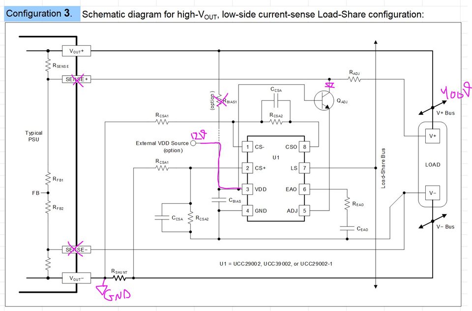
I’m working on a 3 × 1 kW, 385 V DC Output PSFB DC/DC design using the UCC28951 and UCC29002 load‐share controller. In the TI application note, I noticed that the recommended schematic references the UCC29002 GND pin to the load side of the shunt resistor (right side). However, in a previous design, I referenced the UCC29002 ground to the converter side (left side) of the same shunt, and it appeared to work reasonably well. The reason is that the AUX supply is referenced to the converter side.

For my new design with three parallel modules, which grounding reference (load side vs. converter side) is preferred in terms of measurement accuracy, reliability, and ensuring the sense inputs remain in the correct common‐mode voltage range? Are there specific benefits or concerns (e.g., offset voltage, negative common‐mode swing) that would make the load‐side grounding approach more accurate or robust?

Thank you in advance for your guidance!

  • Hello WB, 

    I recommend to tie the UCC29002 GND pin to the load-GND.  

    My reason is that if the IC GND is on the converter side (G2), then variable voltage drop across the shunt resistor from variable load current will modulate the IC GND reference and that may in turn modulate the ADJ current which then may modulate the converter output voltage, which may reduce phase margin for loop stability.
    The GND at the load is a solid reference common to all of the other controllers.  

    Granted that this modulation may be very small, possibly even negligible, but since concern over possible loop interaction can be avoided by tying to the load GND, I prefer to avoid it. 

    By the way, in your purple mark-ups in the first diagram above, you have SENSE+ crossed out. The connection from Radj to Rsense through the VSENSE+ pin is required for load -sharing.  Whether VSENSE+ is an actual connector pin or simply a pcb track, the voltage across Radj must be able to influence the feedback network of your source converter. 

    Regards,
    Ulrich

  • Hello Ulrich,

    Thank you for your feedback.

    This really makes sense to me as well. Colin suggested the other way around couple year ago before he left TI. The reason is that the circuit also includes PSFB Controllers, UCC28951, that are referenced to the left side G1 or G2. Also , AUX PSUs powering up UCC29002 and UCC28951 in each channel are referenced to G1 and G2, respectively. Now, I am not sure if I should reference UCC28951 also to the load ground. If yes, I have to move everything to the right side of the current sense resistor. The measured current will include the load current + all other circuits. 

    As for the RSENSE+, you are correct. This goes back to the PSFB Controller, UCC28951. 

  • Hello WB, 

    I suggest to leave the UCC28951 and AUX grounding as you already have it. No need to move all the GNDs around. 
    This is the way most other designs are and they work fine. 

    Regards,
    Ulrich