This thread has been locked.

If you have a related question, please click the "Ask a related question" button in the top right corner. The newly created question will be automatically linked to this question.

TPS65262-2: INPUT VIN RANGE QUESTION

Part Number: TPS65262-2
Other Parts Discussed in Thread: TPS65400

Tool/software:

Hello TI, 

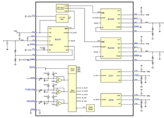
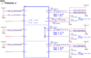
I have a question about the input range of TPS65262-2 VIN1, VIN2, VIN3. 

I checked the input range of 4.5V to 18V in the datasheet, 

but it works without any problem even if I input 5V to VIN1 and 3.3V to VIN2, VIN3. 

Can I use it like this? 

Thank you.

  • Dear Sir,

    I would recommend not and pls follow what the datasheet recommend. It is ensured to work for every device. Thank you!

    BRs

    Lucia

  • Dear Lucia, 

    Could you please tell me what problems can occur when 3.3V is input to VIN2, VIN3?

    Is UVLO corresponding to VIN1?

  • Dear Sir,

    If you look at the block diagram, you can find that LDO input is from VIN1: That might be the reason why as long as VIN1 is above UVLO, even if VIN2 and VIN3 are not over UVLO, you can still have switching behavior of Buck2 and Buck3. I am just curious, not sure the reason that you want to configure the VIN1, VIN2 and VIN3 with different power supply. Is this because you would like to achieve the sequence: make sure Buck2 and Buck3 work after Buck1 output is ready?

    Thanks!

    BRs

    Lucia

  • Dear Lucia, 

    Looking at the block diagram and Figure 7-4(V7V Linear Dropout Regulator and Bootstrap Voltage Diagram) in the datasheet, it seems like there would be no problem if VIN1 is input as 5V and VIN2, VIN3 are input as 3.3V.
    In Figure 7-4, the high-side and low-side mosfet gate drivers depend on V7V and VIN1, and it seems okay as long as there is no problem with UVLO.
    I have already designed the VIN1 input as 5V and the VIN2, VIN3 inputs as 3.3V, so I am reviewing the possibility of a problem.

  • Dear Sir,

    I got your point. In common use cases, I would recommend you can connect Vout to next stage EN pin. You can refer to TPS65400 sequence configuration as as an example:

    BRs

    Lucia

  • Dear Lucia, 

    I wonder if it is okay to input 3.3V to VIN2 and VIN3.
    VIN1 inputs 5V.
    I asked because I checked the block diagram and it seemed like there would be no problem.
    In conclusion, the datasheet spec says that the VIN range is 4.5 to 18V, so I would like to know if it is okay to input 3.3V to VIN2 and VIN3, and if not, what problems will occur.