This thread has been locked.

If you have a related question, please click the "Ask a related question" button in the top right corner. The newly created question will be automatically linked to this question.

TPS7H1121-SP: TPS7H1121-SP: PG simulation

Part Number: TPS7H1121-SP

Tool/software:

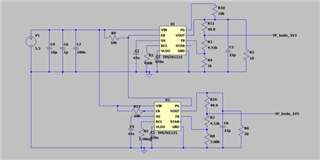
I'm trying to simulate a sequence of 1.5V (1V5) in LTspice, where the PGOOD (PG) signal is supposed to enable 3.3V (3V3) once FB reaches 90% of the reference voltage.

However, PG does not seem to function correctly—it looks like the NMOS tied to PG is always closed instead of waiting for FB to cross the 90% threshold.

Here’s what I expect:

  • PGOOD should be low (0V) at startup, keeping the NMOS closed.
  • Once FB > 90% of VREF, PG should transition high, opening the NMOS and enabling pull-up Voltage

Instead, in my simulation, PGOOD follows an unexpected behavior, and the NMOS seems closed all the time, not waiting for FB to reach the threshold.

Any insights into what could be wrong? Could this be a modeling issue with E_PG_ABM9 or the NMOS switch definition?

Thanks in advance!

 Rocket   

  • Hi Armand,

    Thanks for sharing your schematic. Let me see if I can recreate what you're observing. From there I'll be able to narrow down whether there's a bug we can address or if this is just a simulator netlist syntax issue. 

    Thanks,

    Sarah

  • Hello Sarah,

    Thank you for your reply.

    Could you also test the PG floating? I’m seeing -50V, which makes me suspect it might be connected directly to an op-amp instead of the MOSFET, causing something to float and resulting in infinite gain. 

    Let me know what you find.

    Thanks,

    Armand

  • Thanks for that extra detail Armand. I'll be sure to check that as well. Should be able to get back to you by early next week.

  • Hi Armand,

    Thanks for your patience. I believe there is a floating node bug in the PG feature and have marked this for correction in a revision.

    Can you try making this alteration to the netlist file and confirm that you also see the PG pin function as expected in your simulations? I see the correct behavior with this update: PG being held low until VOUT reaches the threshold and then going HIGH to enable the second LDO. 

    Thanks,

    Sarah

  • More generally, I might also recommend that you slightly alter the EN input for the 3.3VOUT LDO.

    The PG output is not held in a known state until VIN reaches roughly 0.6V. This behavior is not modeled in the SPICE model. The enable turn-on threshold can be lower than the VIN_MIN_PG spec, so with your configuration there is a chance the 3.3VOUT LDO may briefly be enabled by VIN before VIN is high enough to put the PG pin of the 1.5VOUT LDO in a known LOW state. 

    This possible brief early enabling of the 3.3VOUT LDO would probably not be a major issue, but I thought I would bring this up in case it is important for your design.

    Thanks,

    Sarah

  • Hello Thank you for your reply, this seems to work, the PG floating still shows a -50mv instead of 0V but its better then the -50 volts, as for the functionality the PG pin is behaving as expected now, it opens the circuit at about 90-95%. I've tested the simulation and the power sequencing using the PG worked well, Ready for our space mission ;). Thank you 

  • oh i see you mean the 1.5V LDO needs a bit of time to trigger the PG closed so it may be a normally off device and needs to be closed when the LDO has enough power. i thought it was normally on device. is there a way to confirm this? Thank you

  • Hey Armand,

    Yes, that's correct. The internal biasing needed for the open drain PG pin to become active depends on VIN being high enough. So PG will become active (and get pulled low) once VIN reaches that threshold.

    The simplest way to avoid this brief enabling the 3.3V LDO during this period where VIN is rising would probably be to pull the PG pin of the 1.5V LDO up to its own VOUT rail.

    Thanks,

    Sarah