Tool/software:
Hi Sir,
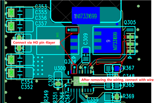
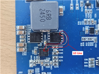
High-side FET and low-side FET behavior is strange.
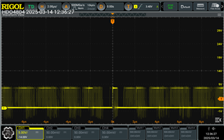
Low side FET gate wave
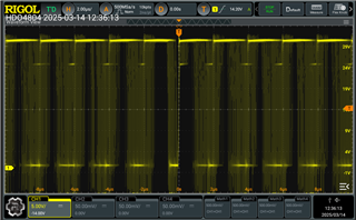
High side FET gate wave
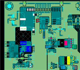
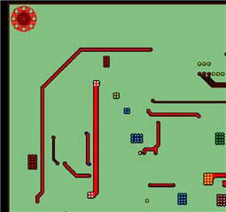
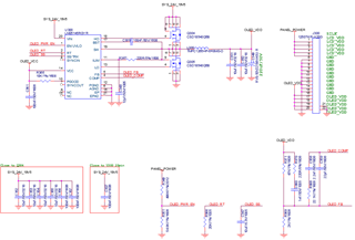
Circuit diagram
Could you please check the problem and tell me how to fix it?
Tool/software:
Hi Sir,
High-side FET and low-side FET behavior is strange.
Low side FET gate wave
High side FET gate wave
Circuit diagram
Could you please check the problem and tell me how to fix it?