This thread has been locked.

If you have a related question, please click the "Ask a related question" button in the top right corner. The newly created question will be automatically linked to this question.

LM5122: High noise on boost SMPS output, not even close to TI webench

Part Number: LM5122
Other Parts Discussed in Thread: PMLKBOOSTEVM,

Tool/software:

Hi

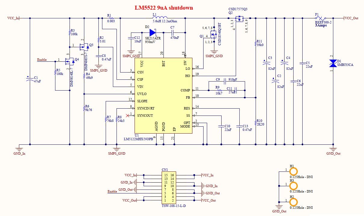
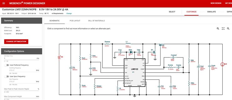
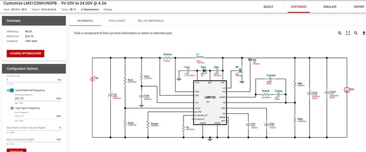
I've used Ti webench to design a SMPS with the LM5122. 

Specs : Battery suply - 8-16 VDC Output 24vdc - 4 AMPS - 30 Celcius ambiant 

This is not very exotic, but this is what I need to do for this project. 

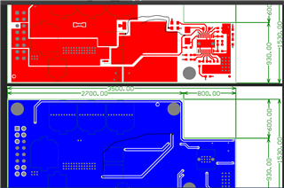
TI webench show 50mV of noise peak to peak, I did try to respect the routing note and the proposed general placement.

I'm aware that the noise can be quite different in real life vs Webench, and I am a 20 year + digital designer , but I would like an active engineer at TI to review my design.

Looks to me that a few components may be missing from this webench design.

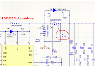
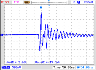
Noise on bare design is more than 3V pk-pk.

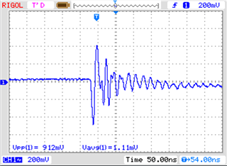
Adding a 100uF cap at the output lower that to 1V pk-pk but it is still very High. Adding more doesnt have as much effect.

Ive seen in the forum that a few person did implement the same design, and they were told to add 100ohms and 100pF on the current feedback resistor. It was quite a challenge to implement, but I did. 

We didnt see any change at all. 

I dont want to restart this part of the design from scratch with another part or another brand at this point, I would prefer having someone from the power management to look at it.

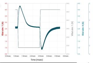
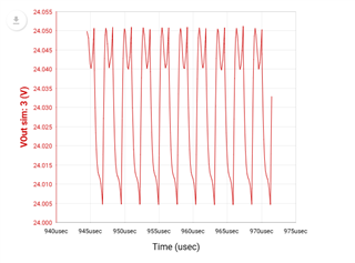
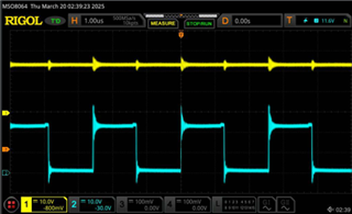
waveform from webench

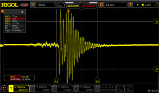
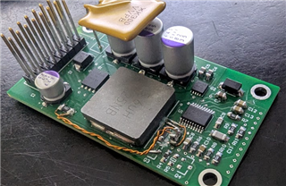
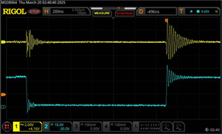
Actual circuit with a 24V out 8ohms load (3 amps)

Thanks

Daniel Pelletier

  • Hello Daniel,

    Thanks for using the e2e forum.
    If I understand correctly, you LM5122 board is running, but shows larger switching noise (or transient overshoots?) than the simulation results?
    I can review your design. Would you be willing to attach the schematic?

    As an additional resource, I can also recommend having a look at the design of our LM5122 EVM boards, which has similar specs as your requirements, and comes with a Users guide including test report.
    https://www.ti.com/tool/LM5122EVM-1PH

    Best regards,
    Niklas

  • Hi Niklas

    Ive added the schematics to this post.

    I did some correction already:

      - I did use a P mosfet to control the LM5522. I would have take some more time analyse the circuit, I would have gone another way since the inductor and the mofset diode will let the 12V go through to the output. I did remove the R%, R3, Q4, Q3 and did a short between the pins 2 and 3 of Q3. I will control the VCC_In from the outside of the SMPS design. The noise was a little bit higher after doing that. I also implement two 100 ohms on each side of the sense resistor R1, going to CSN and CSP, with the addition of a 100pF capacitor. I did use twisted magnet wire. The effect was neglictable. 

    I also see that there is some part around the HO mosfet in some design, but I have no clue about why or what value to implement.

    Q2 show some heat but still acceptable(50-60 celcius) I will improve the thermal dissipation in next version.

    I did bought a PMLKBoostEVM at the beggining of the project, but the since the board was a dual chip design, I did focus more on TI webench design.

    I will give a look at LM5122EVM-1PH.

    How can I share my webench design with you? And is there any reason why the webench design does not recommend any of those parts around the R sense and the power mosfet?

    Thanks a lot for your help

    Daniel Pelletier

    DPe technologies

  • Hi Daniel,

    To share the webench design, you can either print the design to pdf or make a screenshot.
    The RC circuit around the HO MOSFET is a snubber. If you see large overshoots or ringing on the switch node, this snubber is meant to damp these overshoots.
    They are normally not implemented in webench, as overshoots and ringing can come from many aspects which also include layout, so it is impossible calculate suitable snubber values just based on the inputs you enter in webench.

    A common approach for snubbers is to place only the footprints in beginning and then calculate values based on the ringing behavior. A snubber calculator is also provided in the power stage designer tool.
    https://www.ti.com/tool/de-de/POWERSTAGE-DESIGNER

    Another useful resource for validating your component selection is our quickstart calculation tool.
    https://www.ti.com/tool/download/LM5122-BOOST-CALC

    Before looking into schematic optimizations, can you explain once more what the waveform shows, that you shared in the initial post?
    Is this the output voltage?
    And is this just one strong oscillation pulse, or do you see this ringing at every switching cycle?

    It would be helpful if you could take a measurement that shows the switch node signal (voltage at SW) and the output voltage together in one measurement.

    Thanks and best regards,
    Niklas

  • Hi Niklas

    The waveform in my initial post is the ripple from Vout, with ac coupling from my scope. This is a repetitive signal. I will post a new waveform including SW tomorrow when I will be at the lab.

    Thanks for your help

    Daniel Pelletier

    DPe Technologies

  • Hi Daniel,

    Thanks for the feedback.
    I am locking forward for the measurement.

    One additional note I can give is regarding the layout based on the board picture you sent. Q1 is on the left side of the inductor, while Q2 is on the top right side.
    This means the switch node area has to be quite long and may act like an antenna that induces a lot of noise into the system.
    Once we have the waveform picture, we might also review the layout to look for possible root causes there.

    Best regards,
    Niklas

  • Hi Niklas

    Here are the recquired measurments

    Output DC coupling and SW DC coupling
    Output Acoupling and SW DC coupling
    Output Acoupling and SW DC coupling - zoom
    I have added the complete design in pdf
    I did try to replicate the WeBench model within the given space for that board
    Tell me what you think!
    Thanks again!
    Daniel Pelletier
    DPe Technologies
  • Hello Daniel,

    Thanks for providing the measurements.
    The duty cycle looks stable, which is good.

    As expected you see overshoots and ringing on the switch node signal. This is also what it forwarded to the output voltage.
    This not related to the regulation compensation or current sensing.
    Here are recommendations on how to reduce the ringing and stabilize the output voltage:

    - Add gate resistance. (Unfortunately, there are no gate resistors in the current design, so this can only be added after a layout change)
    - Add RC snubber circuit around the high side MOSFET. (In the waveforms you can see at what frequency the switch node signal is ringing. You can follow the steps in the power stage designer to find suitable R and C values)
    - Increase ceramic output capacitance. (There is already C5 and C6 for this, but by adding more low-ESR ceramic caps to the output, more switching noise will be filtered at the output

    As already mentioned, the LM5122 1-phase EVM should be a good reference, also regarding possible layout optimizations.

    Please let me know if additional questions come up.
    Best regards,
    Niklas

  • Hi Niklas

    Thanks for your answer.

    I will do some modification to the circuit and test it. I would like to keep this ticket open until I have new results.

    Thanks again

    Daniel Pelletier

  • Hi Daniel,

    Thanks for the feedback.
    The thread automatically locks after 30 days. Before that, you can reply anytime to re-open the thread.
    Otherwise you can simply create a new ticket.

    Best regards,
    Niklas

  • Hi Niklas

    I did check the LM5122EVM-1PH.

    Its weird to me that the spec are almost the same as the one I need, but the design is very different (parts value and freq) than the one Webench proposed to me.

    I did purchase a sample of the board and I will test it on reception.

    I have tested the snubber on my prototype with the help of the PowerStage designer.

    3 points here:

    1- The tool doesnt tell you the power needed for the resistor. On the LM5122EVM-1PH, its a 3/4W. It would be a great addition. 

    2- The link for the calculation details in the software doesnt work anymore (snubber section). I want to improve my knowledge, can you provide the link?

    3- I did try the method. Initial frew 80Mhz. Added a 4ohms and 1,5nF and did get the freq at 20Mhz, but with almost the same amplitude.

    I was not able to add gate series resistor for the mosfet in my actual design.

    I will see if the Evaluation board show better specs, and restart from there.

    Thanks, and have a good day!

    Daniel Pelletier

  • Hi Daniel,

    Thanks for the feedback.
    1.) Thanks for pointing this out. As snubbers need to support short, but strong current spikes, it is recommended to use higher power ratings here. A rating similar to the current sense shunt resistor is generally recommended.
    2.) The app note for the calculations can be found here: https://www.ti.com/lit/ta/ssztbc7/ssztbc7.pdf
    3.) Please let me know if you achieve better results with the EVM board, or if additional help is required here.

    Best regards,
    Niklas

  • HI Niklas

    I did test the EVM board. The results are quite good, with low ripple on the output.

    Im still curious, so I did a few simulation with webench.

    If I use the same specs as the EV board, the design is quite similar : 10uH, close to a 1000uF on output but without the snubber on mosfet.

    If I use almost the same spec, with the only difference of 4A instead of 4.5, and leaving webench to choose the frequency, I get 5,5uH below 400uF cap on output and 370kHz freq.

    If I force the freq to 250, I get close to your EVM board. I understand that the lower the freq, the more capacitor I will have to use to filter out everything, But even with current sense filtering and snuber, my design wont work when the EVM surely works... I would have like to have another optimization option in webench called "safe design". For sure, this would be my new favorite option.

    I will try to Implement a design near the one from the EVM, it will be hard since it take more space and the physical allocation is frozen. I think we bet too much on the webench simulation on this one.

    Will keep you posted with progress.

    Thanks

    Daniel Pelletier

  • Hi Daniel,

    While the webench tool is very handy for getting design proposals fast with minimal inputs, it can never compare to a reference design that was physically built and tested.
    Even if it takes additional effort, I would recommend to always check if a reference design is somewhere available, as the webench tool is just a calculator after all.

    I will note down your feedback for webench and forward it to the according team.

    Feel free to get back to me if you need a review of schematic or layout of your newest design.

    Best regards,
    Niklas

  • Hi Niklas

    I did a new version of the SMPS

    The results are far from expected. I almost copy the demo board as you can see, even for the parts placement. I have less noise when there is no charge, but the noise is crazy with 3A load.

    I will start to investigate section by section to see what wrong, but I begin to loose faith.

    1538.BoostSMPS_HP.PDF

    I have attached the PDF for your review. You may see something that I didn't.

    I will probably start by removing the mosfet gate resistor as they are 0 ohms on the demo board.

    Ive put way more capacitance on the input, in order to prevent the 12V in to induce noise in other parts of the system. Can it be part of the problem?

    Let me know if you see something.

    Thanks

    Daniel Pelletier

  • I have bypassed the 4.99 ohms gate resistance without any results. I'm not sure where to look next right now.

    Dan

  • Hello Daniel,

    Today is a public holiday in Germany, so I am jumping in and might ask strange questions.

    I expect you are seeing a difference in noise when you use the EVM or when you use your board, right?

    Noise is often injected through the layout and therefore please compare your layout with the EVM layout and check for the specific details.

    Especially the output loop is often a source of noise. Sometimes a small, high frequency capacitor from the output of the top transistor to the GND connection of the bottom transistor might help.

    Best regards,
    Brigitte

  • Hi Brigitte and Niklas

    I have routed my pcb trying to duplicate the demo board layout, within the space available for my board. I did route each sginals and plane in the same way.

    You can compare both pcb using the PDF joined in my last post.

    I also attached to this post a pdf showing the results with different load. The source was a 12V lead acid battery.

    The results shows that my design have a noise 5x to 10x higher than the demo board.

    After those tests, I've added a 0,1 uF capacitor at the postition suggested by Brigitte. The spikes are lower, but the capacitor did not affect the AC waves.

    Im open to any suggestions at this point.

    Thanks for your help

    Daniel

    TESTS RESULTS.pdf

  • Hi Daniel,

    Thanks for all the measurement and layout information.
    As Brigitte already mentioned, I suspect the high noise is coming from the layout.

    Within the layout files, I noticed the following:
    - The RC snubber over the high side MOSFET has a rather long trace, which reduces its effectiveness
    - Can you check if there are any vias on the GND connections of the output side bulk caps?
    I cannot see any vias in the files. If there are no vias to connect the caps to the power stage GND, they can barely provide any filtering.

    Best regards,
    Niklas

  • Hi Niklas

    You are right, I was wong with my output capacitor plane design. I need to add more vias.

    I did modify my proto to be able to continu testing without the need for a new pcb.

    Please take the latest results that I joined to this post as the good one. We will try to improve from those values. Something is wrong with the previous one, as the source was not completely stable.

    We can see that adding a groung path improved both noise at low and high load. I also did change the snubber path and add the capacitor reccommended by Brigitte.

    No load noise changed from 920mV to 464mV

    High load noise changed from 3.18V to 1.10V

    We are way better than before, but still not on par with the demo board (600mV @ 3A)

    My question are as following : 

    - With vias under the output capacitors, do you think the placement is still good?

    - The results seems better with the snubber change, but the 0,1 uF added capacitor was a guest on my side. What value would you reccomend ?

    - What other change can I do to improve the output noise?

    Thanks again for your help, very appreciated!

    Daniel Pelletier

    2025-05-02 Proto 2 Test results .pdf

  • Hi Daniel,

    Thanks for the update. I am glad to hear there were improvements with these changes.

    - With vias under the output capacitors, do you think the placement is still good?
    The placement of C10 and C11 is fine. C12 and C110 are placed further away from the power stage output and therefore less effective.
    However, larger bulks caps have generally higher ESR and are therefore not as good at filtering switching noise as low ESR ceramic capacitors.
    To reduce the ripple, you can consider adding more ceramic capacitance next to C7, where there is still some open space.

    - The results seems better with the snubber change, but the 0,1 uF added capacitor was a guest on my side. What value would you reccomend ?
    The best suitable snubber values can be defined with bench testing. You can unpopulate the snubber and measure the switch node oscillation.
    Then you select values filter at exactly this frequency. We have a snubber calculator within our power stage designer tool for this. https://www.ti.com/tool/POWERSTAGE-DESIGNER

    - What other change can I do to improve the output noise?
    As mentioned on the first question, more ceramic capacitance may be helpful.
    Aside from this, you can also consider running with higher switching frequency, which will reduce the inductor ripple current, but also will increase switching losses.

    Best regards,
    Niklas

  • Hi Niklas

    I will add a more ceramic capacitor on the output as you reccommend.

    I will also try to move the coil to the right by extending the board a little, allowing C12 to be more usefull.

    I will move the snubber over the the Q2 mosfet.

    My question was not clear about the capacitor, sorry for that. It's not the snubber capacitor.

    In her communication, Brigitte mentionned this :

    So ,I've tried with a 0,1uF 50V 0805 between Q3 Ground and Q2 output.

    What would you reccomend for that capacitor?

    Thanks

    Daniel Pelletier

  • Hi Daniel,

    Thanks for the clarification.
    This capacitor has the same function as the other ceramic caps at the output (C5-C8), namely to filter as much switching noise as possible.
    Due to the placement directly at the switching FETs, the filtering effect is the strongest here.
    This is also the reason why I recommended to fill this area with more capacitors in my layout comments to increase both the placement and overall capacitance.

    The lower the series resistance (ESR), the better.

    Best regards,
    Niklas

  • Hi Niklas

    You have here the output of the proto2 without modification:

    And this is with the latest modification:

    To get there, Ive :

    - added the ground strap to simulate new vias under output capacitor

    - Added output capacitor 1x 10uF + 1x 4,7uF + 1x 1uF

    - Move the mofset snubber closer to the mosfet loop.

    To improve more, I have also removed the snuber et redone the subber evaluation process

    - Ive started my design with 8.2ohms - 470pF - believing that the value from the demo board would fit

    -Ive ended up with 1,3 ohms and 6nF

    Since I'm not mastering this part very well, I'm worried about having such values. We have a factor of 7-12x with the demo board. I'm not using the same mosfet(demo board mosfet are obsolete) The noise is lower, but I would like to have your thoughts on this.

    I will do a proto 3, and I will share the design with you before getting it out of factory.

    Thanks again!

    Daniel Pelletier

  • Hi Niklas

    I've attached the new version. I would be please if you can review it.

    Thanks!

    Daniel Pelletier


    3513.BoostSMPS_HP.PDF

  • Hi Daniel,

    Thanks for the update.
    I agree with all your changes.
    The placement of the output caps looks much better now and the bulk caps also have a good GND connection with vias to be more effective.

    One minor thing I can comment:
    I would recommend to place the traces for the MOSFET gates not below the inductor to reduce noise on the driver signals.
    Ideally, you avoid the whole switch node plane.
    This would be an alternative trace for both high and low side:

    I also re-routed the SW pin trance to keep it close to the HO trace to minimize to the loop here.
    You will see the same placement in the EVM reference board as well.

    Best regards,
    Niklas

  • Hi Niklas

    I did the corrections you proposed

    Ive added the corrected pdf for your review.

    The new values for the Snubber looks correct to you?

    I am worry with the very low value of 1,3 ohms.....

    Its also weird to me to have a 3/4W resistor matched with a small 0805 small caps.

    Thanks again for your help!

    Daniel Pelletier

    6840.BoostSMPS_HP.PDF

  • Hi Daniel,

    Thanks for the quick update.
    I like the new gate routing. This design looks good to me.
    The snubber values should be good starting values. I cannot say if these are already the best suitable values for the design, as the ringing of the switch node is very difficult to calculate. Measuring the ringing on bench and then modifying the snubber values to match the ringing frequency should be the most efficient approach here.
    The package sizing is good, even though it feels unnatural.
    I have seen designs in the past that use small packages for both cap and resistor, but these designs did not account for the fact that the current levels running into the snubber can be very high, even if it is for only a very short amount of time, so the resistor broke in these designs.

    Best regards,
    Niklas