This thread has been locked.

If you have a related question, please click the "Ask a related question" button in the top right corner. The newly created question will be automatically linked to this question.

BQ25185: PMIC stuck in pre-charge, 128mA from 640mA

Part Number: BQ25185
Other Parts Discussed in Thread: TPS61023, , BQ25896, BQ25622, BQ25890, BQ25628E, TPS631000

Tool/software:

Hello.

I have a BQ25185 and TPS61023 circuit to charge a large lipo (3700mAh) at about 640mA, but the battery voltage only climbed about 10% (3.79v to 3.89v) after about 3 hours.

I have tried a range of 7v to 15v input, and the results have not changed. 12v would be close to the actual input for our use case. The controller that is powered by the battery is only using about 60mA, and it seems like I'm only getting about 130mA of current into the battery, or about 20% of the expected charge current. The actual resistor value for Vset is reading as about 12.5k instead of 13k. These are what led me to belief that it is stuck in pre-charge. I will attempt to replace the resistor, but advice is greatly appreciated in general.

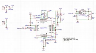
The circuit I am using is the following. Vsys flows into the TPS61023 boost converter to guarantee more than 3.3v for the controller regulator while the charging input is removed. Any advice on what might be wrong here, or a single chip recommendation that can consolidate this circuit, would be hugely appreciated. Thank you.

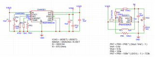
I also seem to be getting 5.7v out of the boost chip instead of 5.0v, but that seems like a separate issue with my resistor quality.

  • Hi Brady,

    Thanks for reaching out.

    It does sound like the issue could be related to the ILIM/VSET resistor. A 12.5k might be setting the battery regulation voltage to 4.05V and ILIM to 500mA.

    Could you try swapping this resistor to 13k and let me know if that resolves the issue?

    Additionally, can you confirm whether the device is in a fault state by checking the status of STAT1 and STAT2? Since these are open drain outputs, it looks like you may need to flip the orientation of your LED on STAT1. Below is an example of how the STAT LEDs are connected in the BQ25185 EVM schematic, which you can find in the EVM User's Guide: https://www.ti.com/lit/ug/sluucs1/sluucs1.pdf?ts=1727795596688&ref_url=https%253A%252F%252Fwww.ti.com%252Fproduct%252FBQ25185

    Best regards,

    Alec

  • Hello, and thank you for your reply.

    It isn't shown in the schematic, but I do have a connection ready for a STAT2 LED, so I will correct the first LED and test the STAT2 pin. Thank you for pointing that out. I don't have a new 13k resistor on hand and am waiting for a replacement, but I can try combining resistors I do have and let you know how that goes.

    If it were setting ILIM to 500mA, shouldn't there still be enough current to charge the battery more than 130mA? I have tried an input of nearly 15v and the total current draw was never more than 100mA.

    Lastly, if I were to consolidate these two and an I2C fuel gauge chip into one, would any of the following be a suitable replacement? I originally went with this combination of chips to guarantee at least 3.4v output whether on wired power or battery power. I believe all of these state that they will enable a boost to 3.51 or greater when a lipo is present OR when the input voltage is present, but I am worried about misinterpreting and getting into trouble with it after more weeks of design and assembly.

    BQ25890, BQ25896, BQ25622

    Thank you, again

  • After some more testing, it seems like there is a sharp change in charging current when I drop the input voltage below 7v. At 5v, I am getting the expected charging current, and the input current does go above 500mA. The datasheet states that it works with voltages up to 25v, but I do not understand why the sudden change above 7v. I do not think we can use it if it is actually working at intended at 12v. Is there an alternative chip that functions well at 12v? I have 3  that we are considering: BQ25890, BQ25896, BQ25622. Thank you for your expertise on this.

  • Hi Brady,

    Thanks for the information. It sounds like the device is entering thermal regulation (TREG) and reducing charge current to prevent overheating. This is almost certainly due to the power dissipation of the device when using higher input voltages and charge currents. It makes sense that lowering the input voltage allows the charge current to increase since the device dissipates less power and stays cooler.

    This is an inherent effect of a linear battery charger. If you're using a 12V input source, a buck battery charger would be more efficient. Those are great choices—if you can share more details about your requirements (e.g., standalone or I2C-controlled), we can help recommend the best fit.


    Additional details if you're interested:

    Refer to section 8.3.7.6 of the BQ25185 datasheet.

    Power dissipation of the BQ25185 depends on charge current and voltage drops across the internal FETs:

    PDISS = [(VIN - VSYS) * (ISYS + IBAT)] + [(VSYS - VBAT) * IBAT]

    Efficiency can be calculated using:

    Efficiency = 1 - (PDISS / PIN)

    To estimate the die junction temperature:

    TJ = TA + θJA * PDISS

    From the BQ25185 datasheet, θJA = 68.3°C/W and ambient temperature (TA) is typically 25°C.

    However, θJA is highly dependent on board layout, so this is just a rough estimate.

    Best regards,

    Alec

  • Ah, that makes a lot of sense. It is a very dense board and linear regulators do get hot. Thank you so much- this problem has been stumping me for days. I was focused on the heat directly from current, and I hadn't even considered the heat from dc conversion. That also makes me feel better about going with one of the buck type charger chips. Right now, I have the BQ25890 as a top choice, but I would greatly appreciate suggestions. Our requirements are the following:

    600-1600mA charging

    Integrated battery level monitoring via I2C would be a big plus (currently using a designated I2C fuel gauge)

    Guaranteed >3.4v Vsys on battery power, so that we can have consistent 3.3v supply for the MCU's LDO

    Small package is a big plus

    Efficient charging at 12v input, but still capable of 5v in case our wall adapter requirements change

    Few external components and low pin count would be better for us. We don't need OTG or USB handshaking at this time.

  • Hi Brady,

    I'm happy to help!

    Based on your requirements, I recommend the BQ25628E. It supports up to 2A output current and an input voltage range of 3.9V to 18V, has no OTG or D+/D- pins, and includes an integrated 12-bit ADC for voltage, current, and temperature monitoring.

    Since SYS is powered directly by the battery in battery-only mode, you may need to consider an external boost or buck-boost converter to regulate your 3.3V rail when the battery voltage approaches 3.3V.

    Let me know if you have any other questions.

    Best regards,

    Alec

  • Thank you for the suggestion. I looked into that one previously and like its features a lot. The integrated buck-boost would be very nice, so I have also put together a draft schematic for the BQ25890. Are there issues I should look out for if I leave the D+/D- pins unconnected, like in this example? Do either have a way to disable output to Vsys? I have a tiny slide switch that I am currently using, which disables the buck-boost chip. I believe disabling the LDO is close enough to the functionality we have, but am curious about options within the charging IC. I considered connecting the CE to the switch, but realized that would only disable charging and not necessarily the output voltage.

    Thank you, again

  • Hi Brady,

    Both the BQ25890 and BQ25628E have ship mode, which is a low quiescent current mode where the BATFET is off, disconnecting SYS from BAT. However, ship mode is meant to be used as a low-power mode when no input source is connected. If you need more control over when you can disconnect your system load, I'd recommend using a load switch solution.

    To clarify, the BQ25890 operates in buck mode from VBUS to SYS but can be configured to operate in OTG boost mode from BAT to VBUS.

    Regarding D+/D- behavior:

    • Leaving D+/D- floating causes the BQ25890 to detect the input source as an unknown adapter, setting the input current limit to 500mA.
    • Shorting D+/D- together causes the device to detect the input source as USB DCP, setting the input current limit to 3.25A.

    Let me know if you have any other questions.

    Best regards,

    Alec

  • Alright, will setting the ILIM resistor or register override the 3.25A limit if D+ and D- are tied together? I would like to avoid putting more than 2A into the battery. Maybe BQ25628E + TPS631000 will be best for our situation, and I can just remove the LDO that we are using. That will consolidate 4 chips down to 2 and keep the circuits relatively simple. The switch can go into the TPS chip enable pin or a separate mosfet to safely disconnect power. Thank you for all of the help.

  • Hi Brady,

    The actual input current limit is determined by the lower of two values: the limit set by the ILIM pin (when the EN_ILIM bit is set to 1) or the value configured in the IINLIM register bits. The ILIM pin function can be disabled by setting the EN_ILIM bit to 0.

    Using a buck-boost with the BQ25628E is a solid approach. Let me know if you have any other questions.

    Best regards,

    Alec