This thread has been locked.

If you have a related question, please click the "Ask a related question" button in the top right corner. The newly created question will be automatically linked to this question.

LMG1020: LMG1020

Part Number: LMG1020

Tool/software:

Hi TI team,

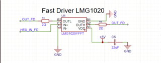
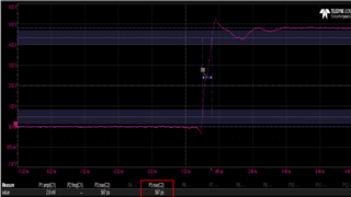
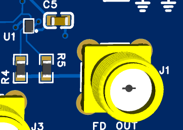
I am using the LMG1020 as a fast rise time driver, and I have attached my schematics and oscilloscope screenshots for reference. The screenshots show a measured rise time with a scope that can measure less than 300 ps.

However, I noticed that the rising edge is not perfectly sharp—there is a noticeable bend in the rising edge, which is not present in the datasheet examples. Could you help me understand why this behavior is occurring? What could be the possible reasons for this deviation? Additionally, if you have any suggestions on improving my circuit to achieve a smoother and faster rise time, similar to the datasheet specifications, I would appreciate your guidance.

Also, if you have an IC that provides an even faster rise time than the LMG1020, please let me know.

Thanks!


  • Hello,

    What transistor are you driving with the LMG1020? The step in the rising waveform may be due to the slight miller plateau region inherent to the transistor.

    Lowering the gate resistance can create a faster rise time but there might be additional over shoot and under shoot that can damage the driver or FET if not handled correctly. Choosing a different transistor with a smaller miller region is another possible option. 

    LMG1020 is our strongest low side dedicated GaN driver and should have the fastest rise time of our products with proper PCB layout.

    Thanks,

    Walter

  • Hi Walter,

    I am not driving any transistor. I am just checking the output at OUTH and OUTL, which are connected to a 2-ohm resistor that is then connected to an SMA connector. Should I remove the 2-ohm resistor, or would you recommend a different approach to improve the rising edge?

    Thanks,

    Ajay

  • Hello Ajay,

    Yes I would suggest removing the 2 ohm resistor and connecting a capacitive load to test. The rise time spec is measured with a 0Ω series resistor and a 100 pF load.

    Thank you,

    Walter

  • Hi Walter ,

    Thank you for the suggestion I will remove 2ohm resistor . Could you please tell me what a capacitive load means by? What I think is if we connect a capacitive load to the signal the Rise time of the signal degrades giving me a slow rise

    Best,
    Ajay Joy

  • Hello Ajay,

    A capacitive load can be a small capacitor placed on the output to simulate a transistor load and is the rise time test condition for the datasheet spec.

    How is the oscilloscope probe connected to the output? The probe should be as close to the gate driver output as possible using a "tip and barrel" ground connection. Parasitic inductance and capacitance in the probe connection and PCB layout can affect the rise and fall time speed.

    Thank you,

    Walter

  • Hi Walter,

    I  connected a 2-ohm resistor to both OUTH and OUTL and then connected them together to an SMA connector. I used an SMA to BNC connector, and then the BNC cable goes to the oscilloscope. Also could you please tell me the reason for the step in the rising edge

    Thank you

    Best regards,
    Ajay

  • Hi Ajay,

    Have you tested with 0 ohm gate resistors? can you also send a picture of the PCB layout?

    Thanks,

    Walter

  • Hi Walter,

    I tried using 0-ohm gate resistors and was able to reduce the rise time by 100 ps. However, the step observed during the signal's rise time remains unchanged, which is my primary concern. I’ve attached a screenshot of the layout for your reference.

    Thanks,

    Ajay

  • Hello Ajay,

    Can you try a smaller VDD bypass cap C5? The device may not be able to draw enough current quickly.

    Thanks,

    Walter