Other Parts Discussed in Thread: TPS54202
Tool/software:
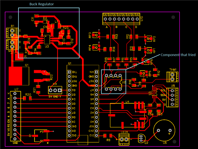
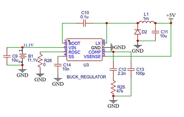
I develop a prototype PCB that included a TPS5405 to regulate voltage between an 11.1V LiPo battery and the rest of the system. I used the following set up for the regulator:
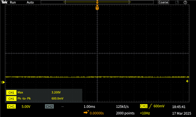
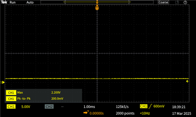
On my first test of the regulator, using a DC Power Supply set to 11.1V it output 5V perfectly as designed. Awhile later, I finally tested it on the actually battery, only for it to output almost no voltage. A possible culprit for the malfunction is an error I made in the design that resulted in an op-amp frying, as after I removed the op-amp from the PCB, the regulator started regulating voltage again, just not correctly. With an input of 6V from the power supply it output less than 5V (1), at around 8V it output 5V (2), and at around 11V it output 3V (3). When connected to the battery it output 2V (4).
(1)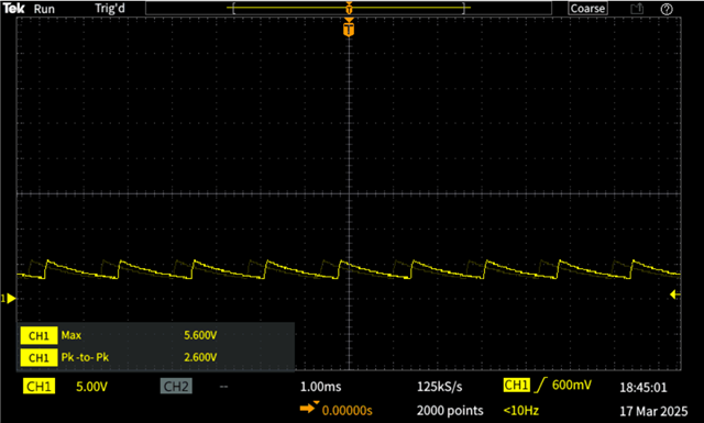 (2)
(2)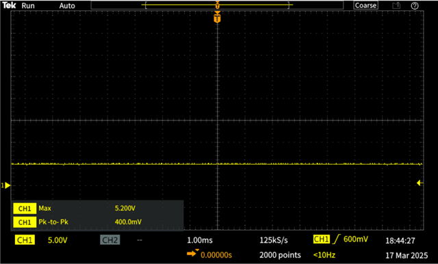 (3)
(3)
(4)
What I'd like to figure out is if the chip itself is damaged and needs to be replaced, or if it's an issue with the supporting RLC network.
I checked each of the pins on the scope while on battery power (I may have gotten some of these out of order):
BOOT: 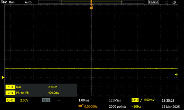 VIN:
VIN: 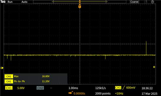
ROSC: (may have mixed up with SS) 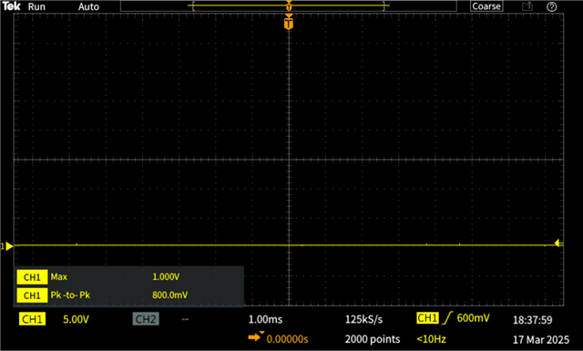 LX:
LX: 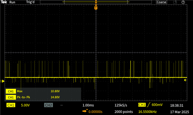
COMP: 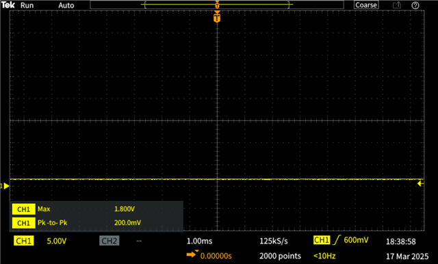
What sort of output should be expected at each pin? Does it seem to be a chip problem or some other issue? What other tests should I run if necessary?
Thank you for your time!
Sara