Tool/software:
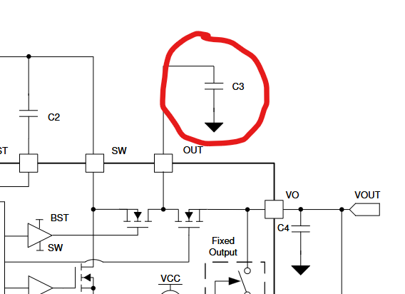
The datasheet for TPS61379 created confusion among its readers when it reused the term "output capacitor" and called pin #10 OUT while simultaneously referring to pin #9 as VO.
Specifically, the output of the boost converter is, technically, pin#10 OUT. It is equipped with external capacitor C3 in datasheet schematics.
Pin #9 VO is simply an equivalent of OUT downstream from a load disconnecting MOSFET. VO pin #9 is equipped with capacitor C4 in datasheet schematics.
Seems to me that the C3 capacitor on the pin named OUT must be quite robust to endure high switching currents, but the datasheet is nearly mute on C3. However the datasheet goes into great detail about the characteristics of C4.
Can anyone provide more guidance on the characteristics of C3? Does the IC's design actually make the ripple on C3 less consequential than I believe it to be?
Jim Olson
Curative Sound
Carmel, IN US