Tool/software:
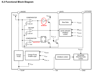
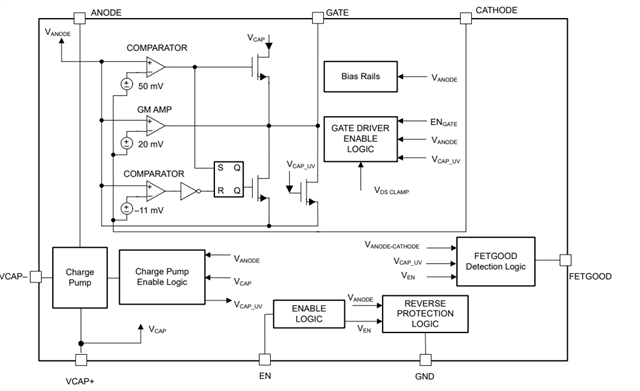
The arrangement of comparators, S/R latch and NMOS transistors driving the GATE output on the functional block diagram (at Section 8.2 of SNOSDD6 – SEPTEMBER 2021) does not appear to be correct.
Specifically it looks like the lowermost comparator, which should cause GATE to be connected to ANODE when CATHODE rises more than 11mV above ANODE, has inverse logic at its output relative to the correct functionality, while the inverter shown between the uppermost comparator and the NMOS that drives GATE from V_CAP, and should cause the full V_CAP voltage to be applied to GATE when the ANODE - CATHODE voltage is large, should not exist. Possibly when the diagram was drawn, the inverter was added into the uppermost output of the window comparator circuit when it should have been added into the lowermost one?