Other Parts Discussed in Thread: TPSM63603
Tool/software:
Hi,
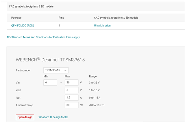
This is Sanjana Renganatha Desigan from QCI. Our team is currently working on a project which requires a DC to DC converter with an input of 12V and the output should be 8V.
We would want that in the form of an eval board so that we can mount in our system and test it. I found under some technical articles that TPS563208 can give up to 8V for a stable input of >=12V, but when I went through the datasheet I'm not sure if this works. Could you please tell me if this work with the required resistor or capacitor changes or is there any recommendations that you could give us for the above specified requirement?
Waiting for your response.
Thank you,
Sanjana Ranganatha Desigan