This thread has been locked.

If you have a related question, please click the "Ask a related question" button in the top right corner. The newly created question will be automatically linked to this question.

LM25183: LM25183 with wuerth WE-IBTI 750342156 Layout questions

Part Number: LM25183
Other Parts Discussed in Thread: LM5180, , LM20242

Tool/software:

Hello TI-experts,

I am designing a dual output power supply with following requierements:

Vin: 16...32VDC

Vout1, Iout1: isolated, 12.1VDC, 300mA max

Vout2, Iout2: isolated, 12,1VDC, 300mA max

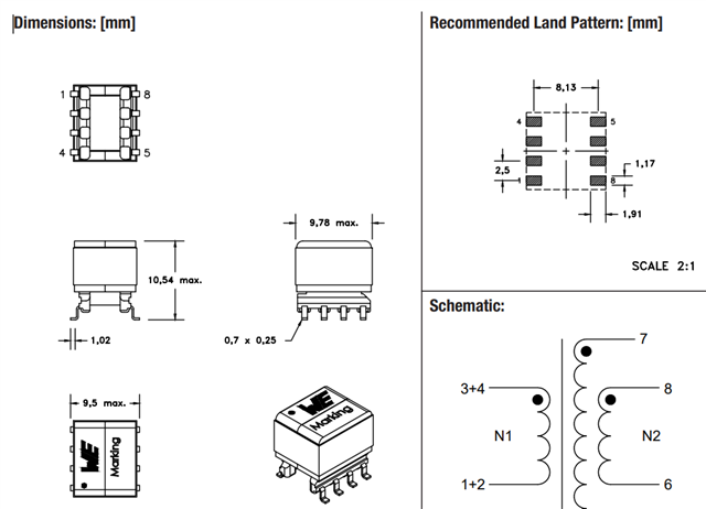
Isolation up to 1,5kV. I will use wuerth  WE-IBTI 750342156 see schematics:     datasheet T1 and its connections: 

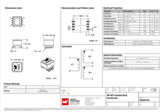
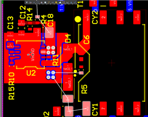
Now with satiesfied interal review, I started routing the board. Since I have a very limited space I am struggeling with the following details:

Placing LM25183 and T1 on top close to each other similar to the eval-board of LM5180 (part of this switcher series) link this 

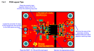
I am struggeling with connecting the switching node pin 1 of the LM close to T1 pin 1 and in the same time with connecting pin 3 of the LM to T1 pin 8. They have to cross each other, which needs to use a second layer to do so: 

  • Would this routing be ok, or should it be changed to another version, where VCC to the Transformer VCC Pin is connected without crossing, but VCC will go arround the LM and its needed components? 

    Another option would be to place the LM and its components on bottom with shortest way and minimum 4 vias per connection to the transformer pins on top? Would this be an option? 

  • Hi Christian,

    -Keeping the switching loop at the primary and secondary side as short as possible is very important for low EMI, better regulation because it avoids layout parasitic. Using vias in the switching loop introduce parasitic inductance which is not optimal. With that being said, my first recommendation is to look for another transformer where VIN and SW pins are place different. You can take as an example 750319029 (WE) from the EVM

    Regarding the option of the bottom layer, I always recommend placing the IC and transformer in the same layer fort he same reason explained below. As a last option, we can place many vias in parallel (like you placed 4) to reduce parasitic inductance.

    Thank you

  • Hi Manuel, Many thanks for you reply and suggestions. What I need to do is a compromiss regarding very limitted space, needing this transformer and routing/ proper EMI-techniques. Well taking another transformer is a good suggestions, but did not find any. How should the 750319029 be used when both secondary windings have to be connected and how to achieve seperation with needed clearance for 1.5kV also between the secondary windings? The choosen transorfmer also delivers the best performance results within the excel-calculators regarding efficency vs. power vs. lower switching frequencies see calculations: 

    I placed and routed with a lot of senetivity the LM and its components on th bottom layer close as possible directly under and the nearest to the transformer SW and VIN pins and used four vias each for SW from top to bottom with low impedance polygon and VCC the same way. Additionally I place a 10uF directly on top as close as possible to VCC transformer pin (end of winding). That is the best I can do for now I think.

    I would appriciate for help finding another transformer for better placing and routing possibilities or axplinations how I can use a transformer with two seconrady windings, which usally used in parallel together for higher output currents separated from each other....

    Many thanks in advance.  

  • Hi Christian,

    Reading the datasheet of 750342156, this is a Flybuck (isolated buck converter) transformer, which means that the pin configuration is designed for it. I recommend looking for a Flyback Transformer (below yuo can see the link for Flyback transformer from WE). I tried looking for a reference design with 750342156 but I did find one. I found this THIS with TI but seems like that reference design is obsolete and does not exist anymore. Below are some recommendations:

    -Reviewing your calculator design, 66uH is way higher the Lmag min recommended. You can decrease Lmag and have more options for a transformer availability with vendors.

    -Please contact WE, Coilcraft or another vendor and they can guide you on a Flyback transformer with your specs. They could also offer you a custom design if needed.

    -Here the link for Flyback transformer from WE ⁣WE-FLYTI Flyback Transformers | Passive Components | Würth Elektronik Product Catalog

    Thank you

  • The TIDA-00123 schematics: TIDA-00123.pdf

    Is the 750342156 not used in this application in Flyback-Mode, because I can not see an additional power inductor regarding buck converters need, or shoud this be L4 with 3.3uH? If it would be the 750342156 woud not work in flyback mode, correct, because air gap to store the energy is missing within this transformer, correct? Wuerth did not respond to my open request on finding another solution...for...two weeks now... 

  • I think I will try 749196111 Datasheet WE-FLEX Flexible Transformer for DC/DC Converter not preffered, but flexible winding-combinations possible

    749196111
  • Christian, thanks for sharing the schematic. Below you can see that 750342156 is used with LM20242 which is a synchronous Buck converter. where the primary winding (1-8) is connected between the SW node and the output. This confirms why the pin configuration is like that. Please use a Flyback transformer from vendors recommended above.

    Thank you