This thread has been locked.

If you have a related question, please click the "Ask a related question" button in the top right corner. The newly created question will be automatically linked to this question.

TPS92611EVM: 9-16Vinput range limitation

Expert 4630 points
Part Number: TPS92611EVM
Other Parts Discussed in Thread: TPS92611-Q1

Tool/software:

Dear e2e support,

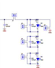
I don't see any obvious reason why our EVM is limited to 16Vin max

Could you tell us more about it? is it just to limit the heat dissipation depending the current and number of leds?

Regards,

  • Hi TISL,

    Our EVMs are designed to withstand the specified operating range outlined in the EVM users guide. Our data sheet for this device has equations to allow the user to configure this device for different input and output specifications.

    You may modify the components in our EVM to accommodate your use case as long as you are within the power range outlined in outlined in our EVM users guide.

    Please evaluate the voltage and current limits of each component placed on our EVM and change them according to your needs. Also, please stay within the recommended operating conditions for the TPS92611 as specified in our data sheet

    Best,
    Daniel

  • Hi Daniel,

    That's exactly my point. 

    Could you explain why the EVM is limited to 16Vin, while the TPS92611 can go up to 40Vin?

    Regards,

  • Hi TISL,

    I answered your question in my previous response. Our EVM was designed using the specifications listed in the user's guide, you can modify it. It was likely designed that way to fit the most common use case anticipated by the designer at that time

    Best,
    Daniel

  • Hi Daniel,

    What do you mean by "you can modify it"?

    What are the hardware items on the board, that we should modify?

    I don't see any component in the BOM which could be a limited factor at the EVM input.

    In other worlds: what should be done on the EVM, to be able to reach the 40Vin?

    Regards,

  • For example, you can remove J1 to attach your own LED load or short LEDs on the board by attaching jumpers to J2, J4, and or J5 shown in the schematic

    Also, you can modify the R(SNS) resistor to change the LED current.

    Please be aware that the your power dissipation will change considerably based on your input and output parameters, and higher input voltages at the same output set points will generate more losses which are dissipated as heat.

    The following information is on page 16 of our data sheet:
    In linear LED driver applications, the input voltage variation contributes to most of the thermal concerns. The
    resistor current, as indicated by Ohm’s law, depends on the voltage across the external resistors. The
    TPS92611-Q1 controls the driver current I(DRIVE) to attain the desired total current. If I(P) increases, the
    TPS92611-Q1 device decreases I(DRIVE) to compensate, and vice versa.
    While in low-dropout mode, the voltage across the R(P) resistor may be close to zero, so that almost no current
    can flow through the external resistor R(P).
    When the input voltage is high, the parallel-resistor current I(P) is proportional to the voltage across the parallel
    resistor R(P). The parallel resistor R(P) takes the majority of the total string current, generating maximum heat.
    The device must prevent current from draining out to ensure current regulation capability

    More generally,
    In linear drivers, a higher input voltage results in more power waste because the excess voltage is converted to heat as the driver regulates the output current. This inefficiency is a fundamental characteristic of linear regulation, where the voltage drop across the regulator is dissipated as heat.

    Here is an example:
    Lets say Vin=16V and we have a single LED with VLED=3V and ILED=100mA. This means there will be 13V across our component and, thus, 1.3W dissipated (as heat) across our driver. Now, if we bump up Vin to 40V and keep the output set point the same, 37V will be across our component, yielding 3.7W dissipation.

    The component's junction temperature is a major concern here as the device will climb approximately 25°C/W. So at 1.3 W, our junction temperature will be around 33°C and if we are operating in an ambient environment of 110°C then we are going to hit our max junction temperature. However, at 3.7W, our device will rise to 92.5°C without exposure to ambient temperature.

    1. Look through our data sheet and our EVM users guide
    2. Find equations to calculate component values
    3. Select parts with the appropriate power ratings
    4. Modify our EVM according to your specifications