This thread has been locked.

If you have a related question, please click the "Ask a related question" button in the top right corner. The newly created question will be automatically linked to this question.

LM5176: Help understanding boost controller problem under load.

Part Number: LM5176
Other Parts Discussed in Thread: PMP21697,

Tool/software:

Hi,

We would appreciate any help understanding the LM5176 behavior in our implementation of a boost controller greatly inspired on the PMP21697 reference design.

Vi: 10-16V

Vo : 42V

Io : 8A max

Fsw : 140kHz

I would include the calculator but we had a lot of problems with the excel file.

Sch :

/resized-image/__size/2756x1741/__key/communityserver-discussions-components-files/196/5241.question.jpg

-> The boost converter works great at no and low loads (<2A out approx). At higher loads the switching becomes somewhat erratic and the inductor heats up quickly.

For debugging purposes, we removed the avg output current limiting and also the hiccup mode.
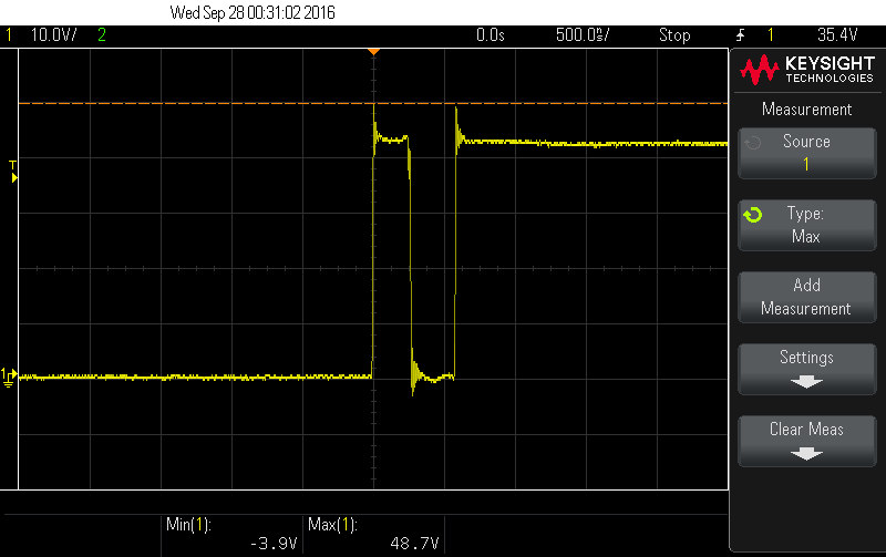
At no load SW2:

And with load exceeding 2A, SW2:

(I am glad I found the reference on this forum to measure using small ground pin on oscilloscope probe)

Any help understanding what is happening would be appreciated.

Also we have omitted the SW2 snubber leg on this design. Could this alone cause this erratic switching?

Regards,

Joseph.

  • Hi Joseph,

    can you explain what issues you had with the quickstart tool - it would be good if you can provide this as well.

    Can we do a review of the layout of the power stage?

    Best regards,

     Stefan

  • Hi Stefan,

    Thank you  for your reply. Yes, please see pictures below (sorry for the quality and rework mess). Please note the RefDes are NOT matching my previously uploaded schematic but main components should be easy to identify.

    By mistake, I initially omitted the two 150R resistors isolating CS and CSG pins. I had to make a contraption using 0402 components pin-mount. It is obvious I will need to re-spin this PCB but I would like to confirm the problems I have come from the inductor current sensing.

    The PCB is 6 layers 2oz. Bottom side is free of components (for direct heatsink contact).

    Again, thank you for your input.

  • Hi Joseph,

    sorry with the images I can not do an layout review. This only shows the top layer and I have not clue what is on the other layer.

    Can you please highlight and mark properly who CS and CSG is connected and routed to the Sense resistor.

    Did you use a Kelvin connection for that?

    Best regards,

     Stefan

  • Hi Stephan,

    No kelvin connections, routing is done via polygons. Top layer for CS and multiple inner for GND (CSG). The size of the sense resistor and the area required for transferring ground current makes the layout pretty tricky.

    Now, for trying to isolate these layout short-comings, I did try to re-route CS and CSG to the sense resistor with wires. Surprisingly, I get the _exact_ same results. I will double check to be certain I don't have any undervoltage event on EN pin.

    Thank you.

  • HI Joseph,

    when re- routing please twist the wires to minimize the impact of disturbances injected into the wires.

    Best regards,

     Stefan

  • Yes, wires were twisted. I will need to clean this board and inspect everything before further work.


    Regards,