This thread has been locked.

If you have a related question, please click the "Ask a related question" button in the top right corner. The newly created question will be automatically linked to this question.

LM5164: LM5164 Qusetion

Part Number: LM5164

Tool/software:

Hi,

I am using the LM5164 buck converter.

Vin = 48V nominal (30V-57V)

Vout = 10.3V

Iout max = 0.1A

Freq = 250kHz

L = 100uH

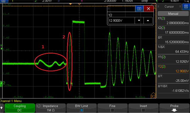
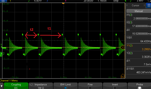
When i decrease the load to ~0.3mA i see the following spike in the SW pin:

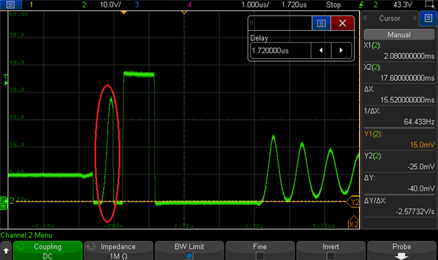
1. Why is that? Is it normal operation?

2. Should i concern about it?

Thank you

Maor M.

  • Hello Maor,

    This is normal discontinuous mode (DCM) operation where the inductor current goes to 0A and the capacitance at the switch node and the inductor resonate.  

    Hope this helps,

    David.

  • Hi David,

    Can you please explain to me for more details the "1" and "2" in the picture? why i get oscillation in "1"?

    2. I see that the times between each pulse in skip mode is different sometimes, is it ok? is it unstable?

    CA = 2.2n

    RA= 300K

    CB = 6.8n

    Thank you

    Maor M.

  • Hello Maor,

    We often see that there may be dissimilar patterns of DCM at light loads, this should not be an issue.

    As for your question regarding section one of the waveform, not sure what is causing this, I suspect it's something on the load side causing this, I highly doubt it to be the converter as both FETs are off during this period of time.  

    Is the converter stable at higher loads, if so, I believe your design is OK.  If not, please share your waveforms and the calculator spreadsheet with recommended values.

    PS: to confirm my comment about it being the load side, measuring the inductor current will give you insight into what is actually going on in section 1...

    Hope this helps.

    David.

  • Hi David,

    1. About section 1, it happens only in very low load (with pure resistor load). So why is it if its pure load resistor? i soldered 1206 resistor very close to the output capacitor (on it).

    2. About section 2, if i understand correctly the oscillation between the inductor and the parasitic capacitance is at the right side of the picture when the inductor current reach 0A. At section 2, it seems like there is start of oscillation and then the lower fet turns on and decrease the signal to 0V and then the upper fet turns on again and we get the big pulse. So, i still don't understand what is section 2 and if i should worry about it.

    Thank you

    Maor M.

  • Hello Maor,

    What is your load doing at this point?

    If you really want to understand what is happening here, suggest measuring the inductor current.   looks like there is current flowing in the inductor, if it were not, it would be ringing as the next cycle.   

    Thanks.

    David.

  • Hi David,

    Please look at the attached picture:

    Orange - SW pin

    blue - inductor current (with wire loop)

    Thank you

    Maor M.

  • Hello Maor,

    Thanks for taking this scope shot.

    it looks like the boot to switch voltage is being charged up due to boot refresh.  This is required to keep the boot to switch voltage elevated and avoided BOOT UVLO being engaged.

    You can check the boot to switch voltage measuring with a diff probe and see it recharging the boot capcitor to avoid boot to switch UVLO occurring.

    Hope this helps.

    David.