This thread has been locked.

If you have a related question, please click the "Ask a related question" button in the top right corner. The newly created question will be automatically linked to this question.

TPS65987DDK: TPS65987DDK Programmer

Part Number: TPS65987DDK
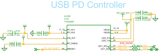
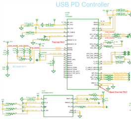
Other Parts Discussed in Thread: TPS65987, TPS25751, TPS65987D

Tool/software:

Hi Christofer, 

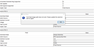
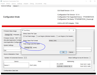
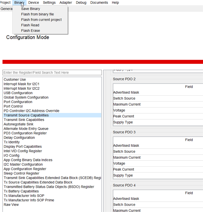
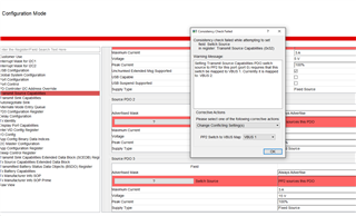
In continues to our conversation, you wrote me in the past that I can use any nominal programmer which use SPI interface for burning the PD controller TPS65987DDK. 

Can you please confirm if the CH341A Programmer can burn image on TPS65987DDK PD Controller? 

Thanks, 

Ohad

  • Hi Ohad,

    Unfortunately I can't confirm if the CH341A programmer will work. You will need to check if it is compatible with the specific SPI flash you are using.

    I can only vouch for the tools I have used, which are the TotalPhase Aardvark and an SF100 dediprog tool. I have never used the CH341A so cannot guarantee it will work.

    Thanks and Regards,

    Chris

  • OK,

    I remember from the first E-mailing I had regard that chip with Aya I think, I was told that any nominal programmer is fine for that job. 

    However, from the examples of "pjt" files I found in the folder given when from downloading the GUI I didn't find a template example file of "Source" configuration. Can you please send me such an example. 

    My E-mail :ohad.fundoianu@gehealthcare.com

  • Hi Ohad,

    I remember from the first E-mailing I had regard that chip with Aya I think, I was told that any nominal programmer is fine for that job. 

    If the nominal programmer supports the SPI flash you are using, then yes, you should be fine for that job. There is no requirement to use the programmers I mentioned above, it is mainly that those are what we happen to have on hand. The CH341 may work, I just cannot confirm as I have not used it before.

    However, from the examples of "pjt" files I found in the folder given when from downloading the GUI I didn't find a template example file of "Source" configuration. Can you please send me such an example.

    For the DDK, if you follow New Project -> 987DDK -> Advanced -> DFP, that should load a good starting point, by setting the number of source pdos in Transmit Source Capabilties to 4, it should set up the transmit source caps message properly for sourcing.

    Here is one generated following similar steps.

    TPS65987DDK_Source.pjt

    Thanks and Regards,

    Chris

  • Hi Chris, 

    1. Does the pjt file you sent is a file for burning through the programmer? 

    2. I didn't succeed follow your steps. I did: New project -> 987DDK -> DFP and then I didn't find the number of Source capabilities.

    Is it possible we could contact on teams and there you can show me where exactly you choose the right parameters for Source mode?   

    Thanks, 

    Ohad

  • Hi Ohad,

    Once you have followed these steps, select Binary->Save Binary.

    Save a "Full Flash" binary to generate the binary needed to load to the SPI flash.

    Thanks and Regards,

    Chris

  • Hi Chris, 

    Thanks for the answer. A few more questions: 

    1. If what I need is 15v at the max then, setting the number of source pdos in Transmit Source Capabilities to 3 is better right ?

    2. I then have gotten this, shall I change there anything?  

    3. Are there any more parameters beside? I got this comment - you didn't tell regard that : 

    Thanks, 

    Ohad

  • Hi Ohad,

    1. If what I need is 15v at the max then, setting the number of source pdos in Transmit Source Capabilities to 3 is better right ?

    Yes

    2. I then have gotten this, shall I change there anything?  

    No, leave as default and genearte by clicking OK

    3. Are there any more parameters beside? I got this comment - you didn't tell regard that : 

    You need to select a save location and file name

    Thanks and Regards,

    Chris

  • Hi Chris, 

    I have followed the steps above and right now it doesn't work. 

    I found that under binary there are some options: 

    If I use a programmer that on the one side is connected by USB to my Leptop and on its other side translates to SPI and then connected by SPI connector to my board with the Flash and the TPS65987DDK, shouldn't I choose "Flash from binary file"  ?

    Ohad

  • Hi Ohad,

    The steps I provided will generate a full flash binary and save it on your PC. Once you have the binary, you need to use your programmer and it's software to load the binary to the SPI flash.

    The "Flash from binary" option is only meant to used with the EVM. It will take a binary and load it to the EVM either through the EVMs FTDI or TIVA interface.

    Thanks and Regards,

    Chris

  • Hi Chris, 

    Thanks, I did exactly the steps you provided and then using the CH341A programmer and its SW I programmed the bin file on the EEPROM W25Q80DV, received indication of "Program successful" but still after shutting down the power and then turn it on, I measured the output voltage on VBUS1/2 and measuring showed '0' instead of 15v as was expected after connecting the Type-C connector.

    Ohad

  • Hi Ohad, 

    Chris is currently out of office. Please allow some delay in responses. 

    Best Regards, 

    Aya Khedr

  • Hello Aya, 

    I have urgent issue and I can not wait till Chris come back from his vacation, specially that he didn't give me the needed required help. 

    I asked for a video conversation since the example he gave me doesn't work. 

    I'm now starting figure what might have made that not working: 

    I connected it on board in a way that PP2 is connected to external 15v and shall be mapped to VBUS2 which sources this 15v to the Type-C connector: 

    According to the error shown above it seems I need to work with PORT 1 instead of PORT 0 in order to be able to map PP2 to VBUS2. 

    I'm not succeeding doing that. 

    Please contact me to show me how to config it on the GUI. 

    Ohad

  • Hi Ohad,

    Please share your latest project.

    It sounds like you may have gotten the flashing to work, but it sounds like there is some misunderstanding on how the part works.

    Do you have an EVM that you have tested with? What is your familiarity with the PD controllers

    At at very simplified level, a PD contract looks like this:

    1. CC lines are biased through resistors to initiate a connection
    2. 5-V is provided for a type-C default contract on VBUS
      1. This needs to be provided through one of the PPHV pins
    3. Once the default contract is negotiated, a PD contract negotiation starts
    4. PD contract
      1. Source advertised Source caps (Transmit source caps)
      2. Sink request one of the PDOs in the Source caps offering
      3. Source Accepts the request
      4. Source prepares voltage (now it could transition from 5->15-V) and sends a PSRDY when prepared to source.

    It sounds like you figured out the original issue regarding flashing. This new issue seems to be an issue with the way you are using the part.

    From the image of the schematic you shared, it looks like PPHV1 is floating, and PPHV2 is connected to a 15-V bus. You have no way to supply the initial 5-V USB-C default contract that is required.

    How do you plan on supplying 5-V and 9-V source contracts?

    For initial testing, if possible, I would recommend removing the 15-V bus and tying it to a 5-V bus to make sure you can at least see 5-V negotiated on VBUS.

    Typically (as with the EVM), the PD controller uses GPIO to control the feedback of the power conversion used for sourcing to supply the desired output voltage.

    From what you have shared, the key issue seems to be the lack of a 5-V source for the default contract.

    Thanks and Regards,

    Chris

  • Hi Chris, 

    I bring here quotes with Aya who was the one who answered me here in E2E 10 months ago while I was doing the design of my Battery board. 

    What you just mentioned now regard connecting 5v for source on PP HV1 was never mentioned by Aya! On the contrary, he told me something totally different when I asked him regard PP HV1. He said that it can act only as a "Sink" which I don't need in my application and therefore it was left unconnected: 

    In addition, in other detailed post specific to that issue, Aya wrote me that 5v comes from PP_Cable pin and that is how I connected the circuit and built the board. 


  • I think we discussed the issues at hand, and the conclusion was that a 5-V supply into PPHV is need for the initial default Type-Contract.

    Please share the pjt when you get the chance.

    I spoke to the team and the TPS25751 currently does not support a source only configuration, so we may keep you on the TPS65987. There are no plans to EOL the device.

    Thanks and Regards,
    Chris

  • BTW - 

    It doesn't work. 

    Could you please review it and advice. 

    Ohad

  • Hi Ohad,

    Was the 5-V modification made? So there should be 5-V on PPHV1 and 15-V on PPHV2?

    I tried your exact pjt on an EVM with a similar setup (5V rail attached to PPHV1 and 15V bench supply attached to PPHV2) and it seems to be working fine there. I can negotiate both 5-V and 15-V.

    Try testing these things first. (I'm assuming you are using the pjt shared above and the 5-V and 15-V connection mentioned in this response.

    1.  Connect a 5-V USB-C sinking device and see if we can at least do 5-V. When you attach the 5-V sink device, does 5-V appear on VBUS?
      1. This could be a phone or a simple type-C peripheral. You could also potentially test with a USB flash drive, although those are typically Type-C only, not USB-C PD. It still would be a good test to at least see if we can source 5-V
    2. Ensure the Flash is being written to properly. If your flash programmer has a read function, read back the flash and make sure it matches the bin file you are using to flash with.
    3. Ensure the PD controller is powered and on. If possible, query the PD controller over I2C. See if you can read register 0x03 and share the payload response. The first 4 bytes of this register are an ascii encoded "mode" register, you should see "APP " mode.
      1. Is VIN3V3, LDO3V3, 5V and 15V up and ready?

    Let me know what the test results work and which ones don't. If you can't test any, let me know as well.

    Ideally, if you have a USB-C PD analyzer that can decode the CC line messages, provide a PD log using this tool so I can review the messaging

    Thanks and Regards,

    Chris

  • Was the 5-V modification made? So there should be 5-V on PPHV1 and 15-V on PPHV2?

    Off-course, I wouldn't check that bin file with no modification. 5V was already stitched to PPHV1 and 15v was connected from first place to PPHV2. 

    Please review again my HW configuration and confirm: 

    Ohad

  • Hi Chris, 

    Regard your suggestions: 

    1. I can measure on my board on the VBUS capacitor which sits just before the connector. This where I always measure and it gives 0v even after connecting 5v on PPHV1 so connecting regular usb2 just for seeing the 5v is not really needed since I can measure VBUS without connecting a usb2 device. 

    2. Regard Flash I will try to find such a tool for comparing write and read files. 

    3. We did not intend to have the PD controller queried by any controller we wanted it to work right after power up automatically and boot. So we didn't connect any interface for read/write registers from the PD controller. 

  • BTW

    I think the HW config in ADCIN1/2 may be wrong, please review it also. 

    Ohad

  • Hi Chris, 

    Let's set a meeting regard that chip today, it's been too long investigation over it. 

    Can you please also advice what is the right HW config from Table 8-5 in datasheet: "Boot mode Pin strapping" for Sourcing from PPHV2/1? 

    Ohad 

  • Hi Ohad,

    Thanks for the feedback. Don't get hung up on the flash reading device.

    It looks like you have BP_No repsonse, safe config? It looks fine. When you power the TPS65987D IC, can you see traffic on the SPI pins? (if you hook up a logic analyzer or an oscope)?

    The EVM has can be used in a similar ADCIN Config and it seems to work fine.

    The boot strapping only really affects the boot up. The Default configs are not recommended to use, and if the PD controller boots properly, it will load the image generated by the GUI.

    I would just like to confirm, the PD iC does have the DK marking on it correct? Your schematic does not appear to specify DK.

    Thanks and Regards,

    Chris

  • Hi Chris, 

    Thanks for the meeting. 

    I sent a summary to Eden which I asked to send you too. 

    I will change the ADCIN1 configuration as you recommended to "BP_NoResponse Infinite wait" (0.1-0.18). 

    The P/N written in that PCB BOM is : TPS65987DDKRSHR. 

    Ohad

  • Hi Ohad,

    Here is the summary from my end:

    1. you will try a different ADCIN Config BP_NO response.

    2. To see if the configs are loading properly, you will try the two projects shared below that enable or disable GPIOs 0 and 1.

         a. TPS65987DDK_Source_meeting_GPIO_0_1_LOW.pjt https://e2e.ti.com/cfs-file/__key/communityserver-discussions-components-files/196/TPS65987DDK_5F00_Source_5F00_meeting_5F00_GPIO_5F00_0_5F00_1_5F00_LOW.bin

         b. TPS65987DDK_Source_meeting_GPIO_0_1_HIGH.pjt https://e2e.ti.com/cfs-file/__key/communityserver-discussions-components-files/196/TPS65987DDK_5F00_Source_5F00_meeting_5F00_GPIO_5F00_0_5F00_1_5F00_HIGH.bin

    If you do not see the GPIOs in the correct orientation after flashing the projects to the board, this likely means that the SPI flash loading is failing somewhere.

    3. If possible, it would be useful to read registers from the I2C port. If you read 0x03 MODE, you should get 5 bytes, which the last 4 corresponding to the ASCII message "APP ".

    Thanks and Regards,

    Chris

  • Regarding a USB Type-C connection and boot process, this is a rough outline of the behavior.

    *Assuming everything is connected properly in HW

    1. Power up the chip through VIN3V3, the Pd controller boots, the controller is in "PTCH" mode
    2. The PD controller reads the ADCIN pins and boots appropriately
    3. The PD controller check it's SPI lines for a SPI flash
      1. If a SPI flash is present, it will attempt to load a configuration from the SPI flash
        1. If the Flash has a bad image, it will get stuck here and stay in "PTCH" mode
        2. If the Flash has a good image, it will load the image and go into "APP " mode
    4. Once the PD controller had booted, a Type-C PD Sink is attached
    5. The connection first enters a Type-C (non-PD) contract, which puts 5-V on VBUS
      1. This 5-V needs to come from PPHV1 (the way the pjt is configured)
    6. Once the Type-C contract is done, the TPS65987 attempts a PD contract
      1. It sends a source caps message according to the configuration of the "TX source caps" register
        1. in this case, it should advertise 5-V and 15-V
      2. The Sink request the highest power it and the source support, in this case we are expecting 15-V
      3. The TPS65987 accepts the request, and begins the transition
        1. In this case 15-V is configured to be supplied through PPHV2, so the TPS65987 will swap the power paths
      4. The TPS65987 sends a PSRDY when it has completed the transition. VBUS should be 15-V at this point.
    7. Done

    Thanks and Regards,

    Chris

  • Hi Chris, 

    Thanks for the project filles. 

    1. I have programmed the GPIO_0_1_LOW and that was enough to verify that the chip is not loaded. I sat with a FLUKE on the GPIO0 resistor which has a PU on the PCB and saw 3.3v value though it should have been 0v according to the project you sent. 

    Then I sat with scope probe on the SPI nets and it seems that signals are running on the lines (CS_n, clk, din, dout) so it seems to work. 

    2. I'm still wondering and asking if there should be any kind of a specific POR sequence involving the HRESET signal in which it should be at '0' for some time and only then '1' and only then the PD Controller will be able to start work ?  I didn't find any evidence for such a requirement in datasheet, can you tell if there is such? 

    3. Regard VSAFE0, what may cause the VBUS transition to near 0 V (VSAFE0V)? 

    4. There is no option to read the register using I2C since there was no intention to develop I2C engine from uC to PD controller which was intended wake up immediately after power up without having any SW involve in it. 

    Thanks, 

    Ohad

  • Hi Ohad,

    1. I have programmed the GPIO_0_1_LOW and that was enough to verify that the chip is not loaded. I sat with a FLUKE on the GPIO0 resistor which has a PU on the PCB and saw 3.3v value though it should have been 0v according to the project you sent. 

    Then I sat with scope probe on the SPI nets and it seems that signals are running on the lines (CS_n, clk, din, dout) so it seems to work. 

    Interesting. So it seems like there is an issue with the EEPROM flash process?

    2. I'm still wondering and asking if there should be any kind of a specific POR sequence involving the HRESET signal in which it should be at '0' for some time and only then '1' and only then the PD Controller will be able to start work ?  I didn't find any evidence for such a requirement in datasheet, can you tell if there is such? 

    No HRESET is not required for the boot process. All that is needed is to update the SPI flash, then power cycle the device through VIN3V3. This is how we typically load new images on the EVMs.

    3. Regard VSAFE0, what may cause the VBUS transition to near 0 V (VSAFE0V)? 

    Any detach's, disconnects, power role swaps, and some resets will require VBUS to transition to 0V.


    For next steps, is there anything we can do to check the flashing process? How confident are you in the SPI flashing tool you are using?

    Thanks and Regards,

    Chris

  • Hi Chris, 

    I really think it is a loading issue and not a program issue. I'm saying that since the SPI flashing tool returns success after burning the flash and also when reading back its content after flashing and comparing to the original file using "Beyond compare" tool the two files are exactly the same. 

    I want to check for next steps if may be the PUs resistors I put on SPI which are 4.7k may be too high though it is very common to use 4.7k for PU. I think it may have some bad effect on the signal because of the SPI loading frequency. 

    Chris I have started examining the recommended replace for tps65987 which is tps25751D and I have some questions about it regard details from Datasheet. 

    I will open another thread for that since it is a different device, however all questions are around one specific issue which is - Can it source 15v/5A ? 

    Thanks, 

    Ohad.  

  • Hi Ohad,

    I really think it is a loading issue and not a program issue. I'm saying that since the SPI flashing tool returns success after burning the flash and also when reading back its content after flashing and comparing to the original file using "Beyond compare" tool the two files are exactly the same. 

    I want to check for next steps if may be the PUs resistors I put on SPI which are 4.7k may be too high though it is very common to use 4.7k for PU. I think it may have some bad effect on the signal because of the SPI loading frequency. 

    Ok, let me know what you can find out. I'm not too experienced with SPI communication so I may not be able to help too much here.  

    I will open another thread for that since it is a different device, however all questions are around one specific issue which is - Can it source 15v/5A ? 

    The TPS25751 is not designed for source only applications. It is mainly meant for DRP and Sink only applications using a Battery Charger.

    If you are not worried about obtaining USB-IF compliance, and this would primarily be in a closed system, yes, the TPS25751 can source 15V/5A and 5V only. It would take some semi-custom json configuration from the team as the part is not meant to be configured for high voltage (>5V) sourcing, but it is possible. It is not possible to obtain PD compliance by sourcing only 5V and 15V. For full compliance, you would need to support 5V/3A and 9V/3A.

    Thanks and Regards,

    Chris