This thread has been locked.

If you have a related question, please click the "Ask a related question" button in the top right corner. The newly created question will be automatically linked to this question.

UCC28C43: UCC28C43DR

Part Number: UCC28C43
Other Parts Discussed in Thread: TL431, , UCC28C53

Tool/software:

Hello,

We use IC UCC28C43DR version for many years without any issues.

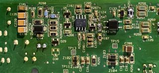
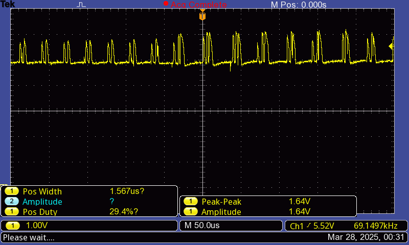
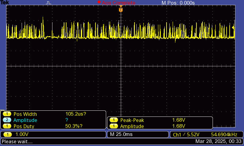
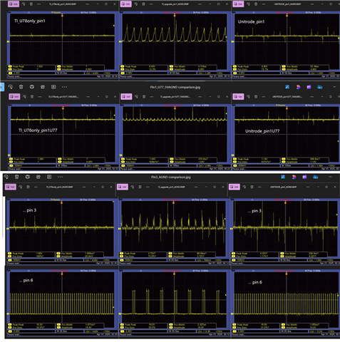
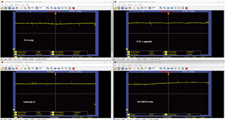
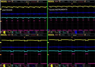
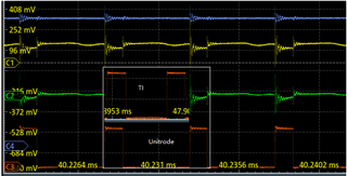
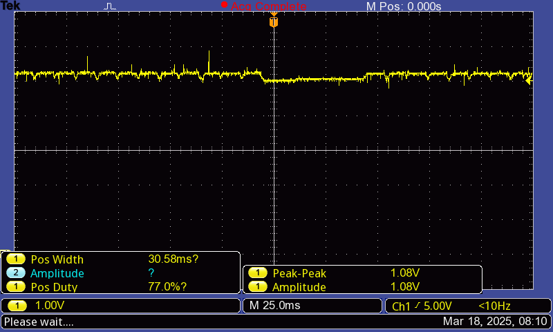
We have ordered new batch in JAN-2025 and we have encountered problems with output voltage → the wave form is not stable (flat), see enclosed pictures as reference.

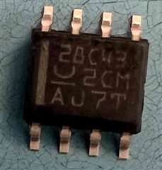
Old version of IC: with marking UNITRODE is working fine.

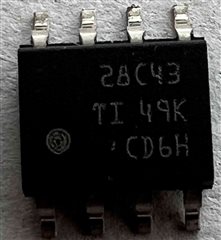
New version of IC: new TI marking (refer to PCN#20211123004.0) → output voltage not stable  

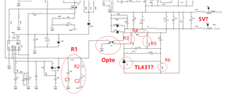
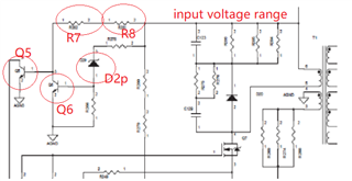
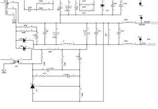
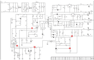
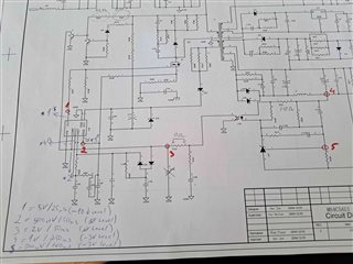
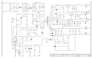
Please see enclosed schematic of application (nothing except IC was replaced) when we have observed problems with output voltage.

Based on TI nothing was changed just the marking.

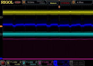
See below 5V wave of problematic IC

Could you please explain the difference?

If you have any questions, feel free to ask.

Thank you in advance for your soon reply.

Kind regards

Peter Torma

  • Hi,

    Please provide all the circled components values. 

    Also, please provide opto CTR value, please confirm TL431 is used, and output = 5V

    We need these to help adjust the design to adapt PCN device COMP max source current 5.5mA

  • Hi,

    Please see below

    Output 5V

    Requested

    Ours

    Value

    R1

    R143

    330 Ohm

    R2

    R187

    10 kOhm

    R3

    R160

    4,7 kOhm

    R4

    R251

    510 Ohm

    R5

    R252

    12,1 kOhm

    R6

    R169

    13 kOhm

    C1

    C154

    0,1 uF

    C2

    C108

    0,1 uF

    OPTO

    U76

    CTR 100-300

    REF

    U77

    HA17431H, 2,5V, 1%

    I hope this will help

    BR // Peter

  • Hi,

    I will have a look and provide the changes needed. 

  • Hi,

    COMP source current needs capable of max 5.5mA for PCN devices. You need to have the below changes.

    -  R1, short across

    -  R4, change to 240 ohm

    R4 = (Vout - Vref - Vopto)/(5.5mA + 1.1V/R3) = (5V-2.5V-1.1V)/(5.5mA+0.23mA) = 240 -ohm 

    -  Remove C1

    I also noticed the below circuit is on COMP so I also need to change these circled. Please provide their values and part numbers. Also, what is the input voltage range which is required to help make chaanges.

  • Hi,

    Please see below table with requested values

    equested Ours Value
    R7 R282 56 kOhm
    R8 R281 56 kOhm
    Q5 Q5 MMBT4401
    Q6 Q6 MMBT4401
    D2p D29 BZX84-C3V9

    Note, that Input Voltage range is 19-60V.

    We use this design for many years without any problems.

    Problems started since we started to use new version of UCC28C43DR (without UNITRODE logo)

    Thank you

  • Hi,

    It is due to the COMP source current max changed to 5.5mA due to not a datasheet specs.

    R7 and R8 = (R282 and 281), total 112k-ohm needs to reduce to total about 85k-ohm, in order to turn on Q5, assuming Q5 hfe = 25 based on its datasheet.

    Please test my suggested values and if still see problems please let me know.

  • Hi,

    Requested changes were performed → 5V output is even worse than before.

    See enclosed wave forms

    Requested Vertiv pos. Value Changes implemented
    R1 R143 330 Ohm R1 (R143) – raplaced by wire jumper
    R2 R187 10 kOhm  
    R3 R160 4,7 kOhm  
    R4 R251 510 Ohm R4 (R251) – replaced to 232 Ohm (two 464 Ohms in paralell – we do not have exact 240 Ohm resistor)
    R5 R252 12,1 kOhm  
    R6 R169 13 kOhm  
    C1 C154 0,1 uF C1 (C154) – removed
    C2 C108 0,1 uF  
    OPTO U76 CTR 100-300  
    REF U77 HA17431H, 2,5V, 1%  
           
    Requested Vertiv pos. Value Changes implemented
    R7 R282 56 kOhm R7, R8 (R281, R282) changed to 42,2kOhm each = 84,4kOhm in total
    R8 R281 56 kOhm R7, R8 (R281, R282) changed to 42,2kOhm each = 84,4kOhm in total
    Q5 Q5 MMBT4401  
    Q6 Q6 MMBT4401  
    D2p D29 BZX84-C3V9  

    BR // Peter

  • Hi,

    It looks there are several 5V output, which 5V waveform you show in your message?

  • Hi,

    Waveforms are the same, there are 2 different time bases - for comparison:

    - 50us

    - 25ms

    The waveform is worse than before.

    I hope it's clear now.

    Any suggestions?

    Thank you

  • Hi,

    Please use the regulated 5V for debugging at this time, i.e., the 5V with the below.

    Please provide a better resolution circuit (prefer in PDF) for better communication.

    Please measure the red dots waveforms. 

    From all support so far, the changes I asked similar to other designs, after made, the designs come to work right away. I am not sure why not this design. So need to check these waveforms to find out.

  • Hi,

    I have sent requested info via private message. 

    Please check and let me know if you need anything else

    Kind regards

    Peter Torma

  • Hi,

    You labeled 1 to 5, but in your waveforms you showed pin 6 - what is pin 6? Is pin 1 in your waveforms number 1 you labeled in the circuit?

    Does "upgrade" mean the circuit after change with my proposed component values?

    It looks you compare the three - please explain each waveform ?

    TI_U78only_pin1_AGND.BMP - TI unit, U78only (?), pin1 (?)

    TI_upgrade_pin1_AGND.BMP

    UNITRODE_pin1_AGND.BMP

    Please provide all waveform explanations to help understand.

    Are these waveforms from no load test?

  • Hi,

    measuring point numbers are just for my information,

    PIN1, PIN3 and PIN6 are pins on IC U78 - UCC28C43 primary side

    AGND - primary ground

    5VA, 5VAGND, PIN1U77 are measuring points on 5V output, respectively secondary side 

    "UPGRADE" means all of your suggestions implemented in circuit.

    TI_U78only_pin1_AGND = only UCC28C43 replaced (all other values are untouched) and waveform is measured on PIN1 of U78 against AGND

    TI_upgrade_pin1_AGND = new TI IC and new suggested values implemented, waveform measured on PIN1 of U78 against AGND

    UNITRODE_pin1_AGND = "untouched" unit, waveform measured on PIN1 against AGND

    All measures were provided under load, 5V feeding LCD display with backlight, some IC as VCC, ..., but the load is always the same.

    Best regards

    Michal

  • Hi,

    It looks the test results without "UPGRADE" are quite the same as Unitrode. So let's remove all my suggested changes.

    The below is from your test results - comparing left to right, they do not make meaningful differences. Please add 5VA_5VAGNF from TI and Unitrode to this to help understand. 

  • Hi,

    Yes, difference between "TI no upgrade" and Unitrode is very small, but there is visible backlight blinking of LCD, respectively small contrast changes

    you can see 5VA against 5VAGND comparison.

    We also tried "upgrade" IC to UCC28C53, and we got same results as with TI UCC28C43.


    Regards

    Michal

  • Hi,

    Again, since upgrade makes worse, so let's remove changes associated to upgrade.

    Please capture the waveforms of "5VA", "U78 pin 1", "U78 pin 6", and "U78 pin 3" in the same picture and in the same time frame since "5VA" slow varying you saw is related to these signals so need capture them in the same time frame to understand which signals causing this varying of 5VA.

  • HI,

    below you can find requested waveforms. Anyway most visible changes are at 10ms/div - also attached, but I am not able to catch these varies in reasonable time frame. 

    It seems that Vout is little bit higher with TI IC

    Legend to oscilloscope channels:

    CH1 = pin 1 (COMP) = YELLOW

    CH2 = pin 3 (ISNS) = LIGHT BLUE

    CH3 = pin 6 (OUT) = MAGENTA

    CH4 = 5Vout = DARK BLUE

    I will send you pictures also via private message in higher resolution

    Regards

    Michal

  • Hi,

    The waveforms are very similar between Unittrode and TI so not able to help find the reasons.

    Can you make the time scale bigger like you said 10ms/div still show these waveforms but with 5Vout variation?

  • Hi, 

    please check private message. It too slow change to catch it, but anyway it seems there is change on PIN1 when Vout is dropping/rising.

    Reagrds

    Michal

  • Hi,

    I replied over there.

  • Hi, 

    replied via PM

    Regards

    Michal

  • Please label each waveform

  • Sorry for that

    Chanel 1 - PIN1 - YELLOW (COMP)
    Chanel 2 - PIN3 - GREEN (ISNS)
    Chanel 3 - PIN6 - RED (OUT)
    Chanel 4 - 5Vout - BLUE (output)

  • Hi,

    Your waveforms show switch frequency is different and duty cycle is different. Did you test on the same physical board? 

    Based on test we have the two devices should have the frequency within 5% but yours is quite more than that. I suspect you used two physical boards to check two IC samples. The frequency can only make that big difference from external RT and CT setup.

    You need to correct this issue first before finding why 5Vout ripple becomes bigger.

  • Hi,

    yes, these waveforms were made on two boards.

    Today I replace chip on board where was assembled TI with UNITRODE chip and the result (except 5V output) is mostly the same, it means different duty cycle.

    Scope set is the same:

    Chanel 1 - PIN1 - YELLOW (COMP)
    Chanel 2 - PIN3 - GREEN (ISNS)
    Chanel 3 - PIN6 - RED (OUT)
    Chanel 4 - 5Vout - BLUE (output)

    Please check PM

    Regards

    Michal

  • Hi,

    I think you need to test on one physical board and using that good board, just replace the PWM controller chip. It looks to me one of your boards has something wrong since the ripple on 5Vout is at pulse off so the energy is delivering from the transformer to Cout. So I suspect your output capacitors on that board have something wrong.