This thread has been locked.

If you have a related question, please click the "Ask a related question" button in the top right corner. The newly created question will be automatically linked to this question.

UC1845A: Selection of gate driving resistence to be connected at the output of UC1845A.

Part Number: UC1845A

Tool/software:

I am using UCI1845A as the flyback controller and the output of the IC is connected to the gate of Flyback main MOSFET through 2.5ohm. The Vcc pin is connected to 13v source hense the peak output current will be 13/2.5= 5.2A. As per the datasheet maximum output current is +-1 A. So what do you think , should we increase the gate resisitence to bring the peak gate charging current less than 1A?? Also what is the purpose of maximum output enery parameter in the datasheet i.e.5uJ. The output energy needed only depends on gate capcitance of MOSFET and charging volatge and that will be less than the specified max rating. Do we have to take care of both the parameters i.e. max output current rating and max output energy rating or either one is fine?

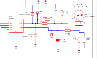
Please find the screenshot of gate driving circuit using the specified IC below:

  • Hi,

    OUTPUT pin 6 has internal resistance to limit the current so no need to consider to limit the drive current externally with the resistance between pin 6 and the gate.

    The specs of 5 µJ is to help to check max capacitance on pin 6. E = 0.5 x C x V^2, for E < 5  x 10^(-6) J, and V = 13V

    C < 5 / (0.5 x 13 ^2) µF = 29.6nF, i.e., you need to make sure pin 6 capacitance less than 29.6 nF, to avoid damage the pin 6. So you need to check your design to make sure based on this. 

    If you have different V, then C can be different, but the check process is the same.

    C roughly is MOSFET Ciss.