This thread has been locked.

If you have a related question, please click the "Ask a related question" button in the top right corner. The newly created question will be automatically linked to this question.

TPS2663: eFuse burns when current limit is reached

Part Number: TPS2663

Tool/software:

Hello

We have included the TSP26633 in a design.

During our initial board bring-up, we have tried to perform over-current tests on the board to verify that the TPS26633 shuts down the current to the rest of the circuit.

Unfortunately, the TPS26633 overheats very quickly as soon as the current limit is exceeded and catches fire within a few seconds. This has now been seen on 2 separate boards.

The load current at which the ICs were burned up was 4.6A, i.e. on 100mA above the current limit threshold.

The load used during testing was an electronic load set to 4.5A. 4.5A was tested for several minutes with a thermal camera, the temperature was at no point over 40°C.

Next test was to increae the load to 4.6A to very shutdown. Shutdown did happen, but during auto-retry the IC started burning.

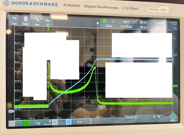
The load capacitance during test was 12mF. The inrush current was also measured at startup (SHDN de-asserted) and this matches very closely Figure 8-4 in the TPS2663 datasheet with an initial peak value of 4.5A

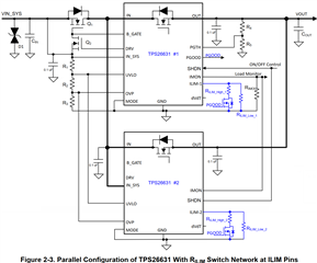
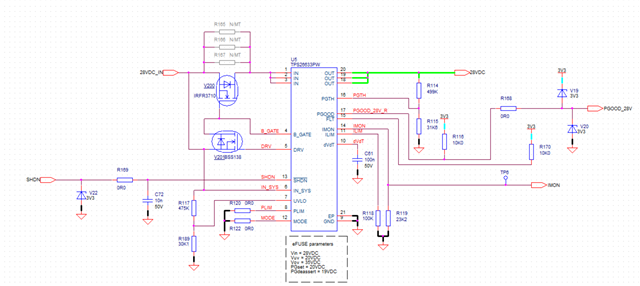
The schematic is shown here:

Please advise as to why this can happen?

  • Hello Lars,

    RILIM value looks to be wrong.

    It should be 4Kohms for 4.5A IOL. Cdvdt value looks wrong.

    Please use below design calculator to determine the values 

    https://dr-download.ti.com/design-tools-simulation/calculation-tool/MD-QV4CzjZsl1/01.00.00.0B/slvc765b.zip

    Please add min CIN of 0.1uF. You can consider adding Schottky diode and some cap near the OUT pin. This is to protect the device from negative abs max.

    Thanks 

    Amrit 

  • Hi Amrit

    Thank you for your fast response.

    I do apologize, I mistakenly uploaded a previous edition of the schematic, that is not representative of the actual board BOM. Please allow me to clarify.

    The value for R_ILIM used for testing is 4.02kOhms. We did however test with C_dVdt of 100nF. Can you elaborate on why this value looks wrong?

    We do have a large Cout of 12 mF bulk capacitance, and it is my understanding that the larger the C_dVdt the slower the ramp up of Vout and the smaller the inrush current. We want to minimize inrush as the application can allow for multiple seconds of charging time.

    Regards Lars

  • Hello Lars,

    Do you have starting load along with the bulk cap?

    Are there any DC-DC converter or circuit you are enabling?

    Please keep min 1.44 uF cap on CdVdT.

    Please check the below app note which has design example of TPS2663 reliable start-up and unknown cap charging.

    Reliable Startup with Large and Unknown Capacitive Loads (Rev. A)

    Thanks

    Amrit 

  • We have two DC/DC converters on the eFuse output. No loads are connected to these devices.

    We also an LDO supplying very little current at 3.3V (approx 30 mA).

    Why would we need add so much capacitance to the CdVdt pin?

    My understanding of the TPS2663 is that it features thermal regulations for powering large capacitive loads at start-up.

    The app note that you refer to has this specific measurement shown in Figure 4-3.

    We have performed a similar measurement which show a very similar result.

    The blue trace is the voltage at the eFuse output and the green waveform is the eFuse input current.

    The initial current spike reaches a value of approx. 4.5A (as programmed with the RILIM resistor = 4.02kOhm), seems to enter thermal regulation and then a second current rise as the eFuse output voltage nears the eFuse input voltage (of 28V).

    From what I can gather, when the TPS2663 enters thermal regulation, the value of CdVdt is no longer relevant as thermal regulation is a separate mode which controls the gate of the internal MOSFET differently.

    This brings me back to my initial question.

    How can it be that the intial power on performs as excepted and shows very similar and predictable performance as compared to the datasheet, but when the output of the device is loaded with a current slightly above the programmed limit in steady state (and strapped to auto retry mode) it burns out almost immediately (one second to a few seconds)?

  • Hi Lars,

    I had the understanding that eFuse failed during start up.

    Thanks for clarifying that.

    Can you capture waveform during that period?

    You can probe VIN, VOUT, IIN and FLt pin.

    There could be abs max violation which caused the device to fail.

    Thanks

    Amrit 

  • We have purchased a number of TPS2663-166EVM boards.

    We have tested with our load and the TPS2663 works as expected.

    We have been able to reproduce the fault on the EVM by removing the input TVS and input capacitor.

    We are now working on making a test PCB of our circuit with the input TVS and input capacitor added and also the output schottky diode added. For this test PCB we want to implement both a single TPS2663 but also two TPS2663s in parallel (we may exceed the 6A load current in our final application). We are implementing the parallel configuration according to SLVAF13, Figure 2-3. However, the AN does not specify where the pull-up voltage of PGOOD is sourced from (since it is open drain). Is it the input or the output of the eFuse?

  • Also, another E2E thread (https://e2e.ti.com/support/power-management-group/power-management/f/power-management-forum/1427130/looking-for-design-file-for-the-evm-of-20a-parallel-solution?tisearch=e2e-sitesearch&keymatch=TPS2663%25252525252525252520EVM#) asks for the design files of the 20A solution mentioned in the AN.

    These were not shared in that thread.

    Can you share them with us?

    Again, I am specifically interested in the pull up voltage to the PGOOD pin, but also the remaining design.

    /Lars

  • Hello Lars,

    PGOOD can be pulled to OUT of eFuse.

    This parallel operation EVM was developed for the evaluation only. EVM is not available for order.

    Are interested in schematics and layout file?

    Thanks 

    Amrit 

  • OK, thank you for that information. My concern is that during an overcurrent event, if the output voltage will fall during the period of the pass FET TPS2663 when it isn’t enhanced. Can the output voltage be reduced to the point where the PGOOD pull-up voltage isn’t high enough to enhance the external NMOS (causing R_Ilim_high to not be switched in). Is this a realistic scenario?

    We are primarily interested in the schematic, we would like to receive the layout as well if possible. Specifically, I am interested in the NFET, is it recommended as logic level or not. Any recommendations for this FET?

     Thanks in advance!

  • Hello Lars,

    When TPS2663 is not enhanced PGOOD signal will be asserted to GND.

    After successful start-up only PGOOD signal will be high and RILIM will be set.

    Find the FET recommendation below for Q1 and Q2 external FETs.

    Thanks

    Amrit 

  • I am aware of this. But since PGOOD is an open drain outout, the voltage at the PGOOD pin is sourced from the output voltage (given Vout is used as the pull up voltage source).

    I am aware of the Q1 and Q2 FETs. I was specifically thinking of the two FETs for Ilim switching.

    We propose to use the BSS138 as the two switching FETs and place a zener diode (e.g. 12V nominal) atthe PGOOD pin (to clamp the gate-source voltage to a value less than Vgs,max of the BSS138). This scheme relies on the output voltage being at least 3-4V when the TPS2663 pass FET is enhanced in order for the PGOOD pullup voltage to be high enough to enhance the switching FETs. Do you agree this is a possible solution?

    We are still interested in the schematic and layout files of the 4-parallel evaluation board. Are you able to share these?

  • Hello Lars,

    Yes, I can share schematic and layout. I have sent you a request. Please send a private message.

    I will share over mail.

    Thanks 

    Amrit