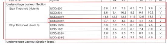
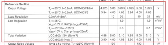
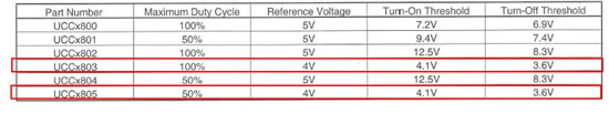
I would like to know where the threshold values are taken from. Are they a comparison between the comp output and the Output of chip? If not, where are they determined from?

-
Ask a related question
What is a related question?A related question is a question created from another question. When the related question is created, it will be automatically linked to the original question.