This thread has been locked.

If you have a related question, please click the "Ask a related question" button in the top right corner. The newly created question will be automatically linked to this question.

TPS274C65: Unpowered device affects the SPI bus

Part Number: TPS274C65

Tool/software:

Dear support team,

On our custom pcb board are four TPS274C65 chips connected to the same SPI bus. Two chips are using their internal voltage regulator where the VS input is supplied by +24V and protected by an eFuse. The other two chips are supplied by an external +3V3 voltage regulator through their VDD pins. Their VS inputs are also supplied by +24V and protected by an eFuse.

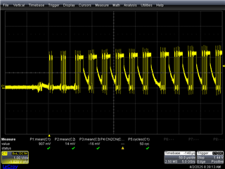
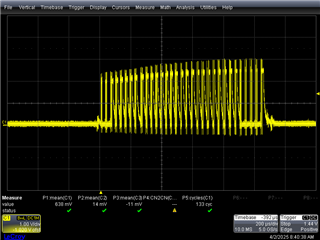
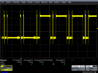
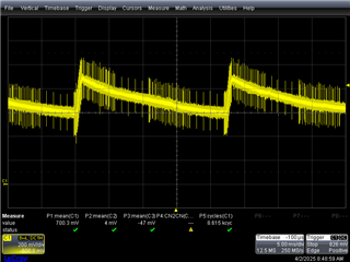
The SPI communication between the microcontroller and the TPS274C65 chips works correctly when all four chips are powered. If a TPS274C65 chip with internal voltage regulator has no VS supply, it will affect all other active TPS274C65 chips on the same SPI line so that they won’t work correctly. This unsupplied chip will probably pull down the data signal of the MISO line. In this case, a high-level signal transmitted by an active TPS274C65 chip won’t exceed the high-level voltage threshold of the microcontroller and therefore won’t be validated correctly.

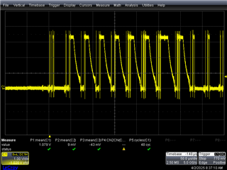
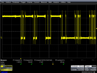
If the two TPS274C65 chips aren't supplied with power, there will be a voltage drop on the MISO line of at least 300 mV compared to the signal where all four chips are supplied with power.
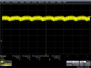
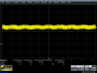
This voltage drop dpends on the amount of the data traffic on the MOSI line. With a small amout the high level is around +2V and with a large amout around +3V.

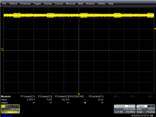
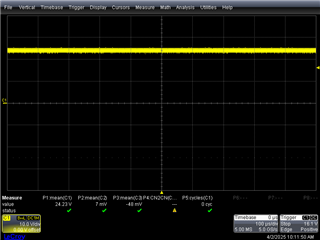
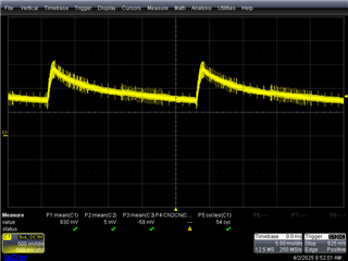
The measurement of the voltage signal at the VDD pin of an unpowered TPS274C65 chip shows a capacitive charge and discharge signal up to +2V with a frequency period, that corresponds to the SPI communication poll time.

Is this a desired/known behaviour of the TPS274C65 chip?
What solution is recommended to avoid this behavior?

Thanks in advance.

Regards,

Aron

  • Hi Aron,

    Are you using a ground diode // resistor network for reverse polarity for these devices?

    And, what voltage shows up on VS when you see 2V/3V on VDD? Can you send a waveform of MOSI, VDD, and VS?

    Thanks,

    Patrick

  • Hi Patrick,

    yes, ground diodes are used and the eFuse for the TPS274C65 chips with the internal voltage regulator is the TPS16630RGER.

    The measurements of the following waveforms have been done with a SPI clock frequency of 2.5 Mbit/s.


    Waveforms of signals where all four TPS274C65 chips are powered:


    MISO signal of a SPI data transfer. The high level of the signal reaches +3.3V.

    MOSI signal of a SPI data transfer. The high level of the signal reaches +3.3V.

    VDD signal of a TPS274C65 chip with the internal voltage regulator. The voltage level of the signal is +3.3V.

    VS signal of a TPS274C65 chip with the internal voltage regulator. The voltage level of the signal is +24V.


    Waveforms of signals where the two TPS274C65 chips with the internal voltage regulator are disabled:


    MISO signal of a SPI data transfer. The high level of the signal only reaches +2V at the beginning of the transfer.

    MISO signal of a SPI data transfer. A data packet sequence is transmitted. The high level of the signal is initially at approximately +2V and increases up to +2.5V towards the end.

    MOSI signal of a SPI data transfer. The high level of the signal reaches +3.3 V and isn't affected by the two unpowered TPS274C65 chips.

    VDD signal of a TPS274C65 chip with the internal voltage regulator. A SPI data packet sequence is transmitted every 10 ms, where every second sequence contains a larger data packet. This transmission interval of the larger data packet corresponds to the frequency of this capacitive charge and discharge signal (~20ms). The peak voltage level is approximately +1.5V.

    VS signal of a TPS274C65 chip with the internal voltage regulator. A SPI data packet sequence is transmitted every 10 ms, where every second sequence contains a larger data packet. The peak voltage level is approximately +1V.

    VDD signal of a TPS274C65 chip with the internal voltage regulator. A SPI data packet sequence is transmitted continuously. The peak voltage level is approximately +2V.

    VS signal of a TPS274C65 chip with the internal voltage regulator. A SPI data packet sequence is transmitted continuouslyThe peak voltage level is approximately +1.5V.

  • Hi Aron,

    Thanks for the detailed response. What's probably happening here is that the SPI signals are propagating through the ESD diodes to VDD then from VDD across a diode drop to VS, so this turns into a situation where the SPI signals are trying to charge whatever capacitance is on VDD and VS. Could you test this again while shorting the ground diode?

    Also, do you keep the nCS signal low all the time, or do you only pull it low for SPI packets?

    Thanks,

    Patrick

  • Hi Patrick,

    thanks for the information. The nCS signal is only pulled low for SPI packets.

    With ground diode do you mean the "Optional Reverse Polarity" circuit of the Typical Application (Figure 9-1) in the data sheet?


    If this is the case, we have not connected a ground diode/resistor network to the devices. We just connected a diode in reverse bias to the power supply (anode: GND, cathode: Vs).

    BR,
    Aron

  • Aron,

    Just for clarification, are you using the device in daisy chain SPI mode or addressable SPI mode? 

    Best Regards,
    Tim

  • Hi Timothy,

    the devices are communicating in addressable SPI mode.

    BR,
    Aron

  • Aron,

    I am discussing this internally to see what could possibly be the program here. Apologies for the delay.

    Best Regards,
    Tim 

  • Hi Tim,

    ok, thank you for your effort.

    BR,
    Aron

  • Aron,

    Just to give an update here we are meeting with the design team for the part on Monday to go over and clarify this. I do not see anything that would explicitly cause the voltage drop, however I am checking with the design team for exact details on what the internals of the pin looks like. 

    Best Regards,
    Tim 

  • Hi Tim,

    have you found out anything new about this behavior or do you have any information about the current status?

    BR,
    Aron 

  • Aron,

    Sorry for the delay in response here. After checking with design, there is a 1Mohm passive pull-down on SDI, SDO and SCLK. This would explain the lines being pulled slightly down when the pin is unpowered.

    Best Regards,
    Tim

  • Hi Tim,

    the SPI lines SDI and SCLK aren't affected by the two unpowerd TPS274C65 chips. This doesn't explain why only the SDO line is pulled low.
    Can you please explain in detail the cause of this behavior?

    BR,
    Aron

  • Aron,

    I am trying to see if there is something passive in the device that would cause a pull-down specifically on SDO and not the other lines. Right now we are not seeing anything in the design, however we are looking to see if there are any other paths to ground.

    Best Regards,
    Tim 

  • Aron,

    We have been looking through the design and can't find anything specifically special about the SDO pin during the unpowered state. Specifically, you are talking about SDO (MOSI), correct? The only passive component that we would see when the device is unpowered on this line is the 1M pull-down resistor... which does not seem to be affecting the system,.

    Best Regards,
    Tim

  • Hi Tim,

    the voltage drop occurs on the data line output (SDO) of the TPS274C65 device (MISO of the SPI interface). I'm not convinced that a 1M pull-down resitor could be the main reason for this behaviour, but thank you very much for your research and the information.

    BR,
    Aron