Tool/software:
Hi Team,
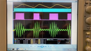
Would you please share the light load operation mode with me? I can NOT find the light load operation conditions/mode introduction at datasheet.
Are this PFC/PWM controller support burst mode?
Thank you.
Tool/software:
Hi Team,
Would you please share the light load operation mode with me? I can NOT find the light load operation conditions/mode introduction at datasheet.
Are this PFC/PWM controller support burst mode?
Thank you.