This thread has been locked.

If you have a related question, please click the "Ask a related question" button in the top right corner. The newly created question will be automatically linked to this question.

UCC28782: About UCC28782BDLRTWR

Part Number: UCC28782
Other Parts Discussed in Thread: LMG3622, STRIKE

Tool/software:

Hello,

I am an FAE at a distributor that handles TI products.
I have received some inquiries about UCC28782BDLRTWR from my customer.
(Question 1)
This is a question about the protection operation of the FLT pin.
Across the entire load range, latch-off is required to protect against output overvoltage, etc.
I was considering a configuration in which the FLT pin is pulled down by a photocoupler signal.
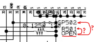
However, during board evaluation, when pulled down with a switch as in the attached Fig. 1, latch-off can only be achieved in AAM mode.
Other modes operate normally.
Is this operation correct?
Also, if the FLT pin cannot be used, I am considering a circuit configuration in which the CS pin is pulled up from REF as in the attached Fig. 2. Is this OK?
I would appreciate any advice or cautions.

(Question 2)
There are areas where the operating waveform is unstable depending on the input voltage and load current values.
This phenomenon occurs particularly at high input voltages or light loads.
Attached are waveforms for input voltages of 100V and 240V, and load currents of 7A and 12A.
Look at the light blue Trans pri. Also, please let us know if ZVS is working properly.
Could you please tell me what causes the operation to become unstable and what solutions there are?

Best regards,

UCC28782.pdf

  • Kaji,

    Can you please share the schematic with us? We will look into this.

    In the meantime, is there a TI FAE who is in the loop as well?

    Best,

    Ning

  • Thank you for your reply.
    If I get a circuit diagram from my customer, is it possible to email it to you privately?
    Additionally, this matter is being primarily handled by the distributor, so TI FAE is not involved.
    Best regards,

  • You can involve TI FAE y-ishii@ti.com to channel schematics to us.

  • Thank you for your reply.

    Once I get the circuit diagram from my customer, I will contact ishii-san.
    Additional information from my customer.
    Question 1 has been resolved. Thank you.
    Regarding Question 2, the unstable operation may be affected by the Dither function.
    The dither function can be disabled when IVSL is lower than 580uA, but this was intentionally set and verification was performed.
    As a result, it was found that unstable operation was reduced.
    However, this measure cannot be implemented due to the customer's specifications.
    Also, my customer wants a LATCH for the FAULT, so UCC28782A cannot be used.
    So, if there are other ways to disable Dither or reduce its effects, please let me know.
    It seems that the dither amplitude changes depending on the output voltage. Is it possible to use this? How to make the output voltage appear lower, etc.
    The customer's specifications are as follows.
    (Specifications)
    VIN: 100V to 240V
    VOUT: 20V
    Output power: 65W

    Best regards,

  • Hello Kaji-san, 

    This controller is used in a number of successful designs with the same kind of input and output specifications.

    The waveform of  VIN = 240V and Io = 7A shows signs that suggest that there is significant ripple voltage on the secondary side of the transformer. 
    I suspect this design uses secondary-side resonance and there may be in sufficient damping of the secondary filter resonance.  The filter resonance is different than the ACF resonance, but if it is undamped, the frequency dithering might be aggravating it at high line and lighter loads. 

    The dithering function of UCC28782 cannot be disabled.  But if proper damping can be ensured then the dithering feature should not be a problem. 
    To reduce the dithering effect, it is possible to fool the controller into "thinking" it is controlling a low voltage but then the peak power levels will also be affected and output OVP is defeated.  It is preferable to do a normal design and ensure stability through proper damping and feedback compensation. 

    We shall wait for the schematic file to arrive to investigate this further. 

    Regards,
    Ulrich

  • Thank you for your reply.
    I received the circuit diagram from my customer, so I will send it to you via ishii-san.
    This contains some Japanese text, but please let me know if you have any questions.
    Also, all resistance units are in Ω.
    There is one correction.
    The output voltage was 5.1V. Sorry.
    Best regards,

  • Hello,
    Have you received the circuit diagram?
    If you have already received it, I would appreciate it if you could let me know.
    Best regards,

  • Hello Kaji-san, 

    I confirm that I have received the schematic file this morning by way of Mr. Ishii-san.  Thank you very much. 

    I scanned through it briefly and request the following additional information to help me with analysis:
    1.  What is transformer T101 magnetizing inductance?
    2.  What is transformer T101 primary leakage inductance?
    3.  What is inductor L201 inductance?
    4.  On IC503, please clarify if R501 is OPEN or if SP502 is OPEN (see snippet, next):

    Regards,
    Ulrich

  • Thank you for your reply.
    I will contact you with the reply from my customer.

    1. What is transformer T101 magnetizing inductance?
    ⇒88.1uH (actual measurement)
    2. What is transformer T101 primary leakage inductance?
    ⇒2.1uH (actual measurement)
    3. What is inductor L201 inductance?
    ⇒0.753uH typ.
    4. On IC503, please clarify if R501 is OPEN or if SP502 is OPEN
    ⇒R501 is open. SP502 is connected.

    Best regards,

  • Hello Kaji-san, 

    Thank you for the information. 

    I am concerned about R501 being open-circuit.  
    Without R501, I don't know what kind of current-sense signal is conveyed to the UCC28782 CS input. 

    Using rough estimates, I calculate that peak primary current at low line would be around ~2.4Apk, so IC503 CS output current would be about ~1.66mA.
    For a 0.6V signal at UCC28782 CS input, R501 would be about 0.6V/0.00166A = 360ohm.  
    The actual values may be different than this estimate, but I think R501 should have some appropriate value.  I don't think it should be open. 

    The output LC filtering components appear to be unconventionally large to me.
    These values may have some influence on the unstable waveforms seen in the "UCC28782.pdf" file posted above.
    Is this ACF intended to operate with primary-side resonance, or with secondary-side resonance? 

    This Excel-based Calculator tool should be used to optimize the ACF design:
    https://dr-download.ti.com/design-tools-simulation/calculation-tool/MD-llLhPpwTJt/01.00.00.0C/sluraz0c.zip

    Regards,
    Ulrich

  • Thank you for your reply.
    I will let you know the information I confirmed with my customer.
    First, the design is done with secondary side resonance.
    Secondly, regarding CS, the 120 Ω of R561 is Rcs, and the 470 Ω of R558 is Ropp.
    Therefore, R501 can be left open. Just to be sure, I'm currently checking with our customers about the role of R501.
    Best regards,

  • Hello,
    I would like to share some additional information with you.
    There is no particular purpose for R501, but I have created the circuit diagram so that Rcs can be placed very close to the CS pin of the LMG3622.
    In the current specifications, R501 is open, and R561, which is placed closer to IC501, is used.
    Also, for reference, the customer would like to know how to calculate 2.4Apk.
    Finally, please let me know if there are any optimal constants for secondary side resonance.
    Best regards,

  • Hello Kaji-san, 

    Thank you for clarifying this question. 

    I did not even see R561 until you brought it to my attention.  I saw R501 at IC503 and I saw R558 at IC501, and I thought those two were Rcs and Ropp.  
    I did not think to look for a "second" Rcs (R561), so I completely missed it. 
    It makes sense to me that your customer provided two options for Rcs locations and chose to populate R561, close to the ACF controller. 

    I can proceed to analyze the schematic diagram component values, but I may need a day or two to accomplish this.  I have to interleave this with other tasks. 

    For the rough 2.4Apk estimation, my thinking is as follows:
    1.  65W output at 94% efficiency = 69W input at 90Vac.  
    2.  Bulk voltage at 90Vac = 127Vpk.  Ripple is very low with 440uF bulk cap, so assume ~115V average.  
    3.  69W/115Vavg = 0.6A avg current to the transformer.  
    4.  With transition-mode operation and assuming roughly 50% duty cycle, peak primary current = 0.6A/0.5/0.5 = 2.4Apk. 

    This is a crude, quick estimation of the current.  Actual peak current depends partially on a few other factors, but mostly on the actual duty cycle. 

    Regards,
    Ulrich

  • Thank you for your reply.
    I understand that analyzing the components in the circuit diagram takes time.
    It's okay if it takes time to analyze the circuit constants, so I would be very grateful if you could give me your opinion on the constants of the secondary side resonant circuit.
    Best regards,

  • Hello Kaji-san, 

    Since this is a public forum and the schematic was provided to me in private, I don't want to divulge too many specific details about the design here.

    In general, this design is very "generous" with capacitances given the relatively low power level required. 
    The resonant capacitance is too big, in my opinion, and the output inductor is not matched properly and is underdamped.  

    There are other aspects of the design that could be improved, but it depends on what changes are allowable. 
    How much flexibility is there in the transformer design, for example?  Different turns-ratios? Different magnetizing inductance?

    I recommend for your customer to fill out the Calculator Tool with their design targets. 
    I have done so in a local file here using the component values from the schematic and adjusted some of the target values until the tool recommended those same values used in the schematic. 
    The most notable result is that the lowest switching frequency is much lower than I would recommend. 
    (For UCC28782, I recommend fSW(min) > 100kHz, for example.  Probably higher to take advantage of the GaN switches, compared to Si FETs. )

    I could make some assumptions on this design to suggest improvements, but I prefer not to guess at what your customer wants or needs.
    That's why I think it will be very helpful for your customer to fill out the Excel Tool, and I can help with inputs that are unclear or unknown. 
    Much of the specifics will probably have to be done outside of this public forum, but I can give generalized advice here for the sake of other readers.    

    Regards,
    Ulrich

  • Thank you for your reply.
    The customer is currently reconsidering the constants using your Excel calculation tool.
    Once we receive the results from the customer, we will report back to you and would appreciate your feedback at that time.
    You say that in the secondary resonance, the resonant capacitance is too large and the inductor is not properly matched.
    For reference, could you please tell me the constants Co1 and Lo that you calculated for the current circuit?
    Also, it seems that customers can change the transformer.
    Best regards,

  • Hello Kaji-san, 

    Please find attached here the UCC28782 Calculator file with my suggested implementation values for to achieve the design targets previously listed above.
    UCC28782 Calculator RevC PAN.xlsx

    Many aspects of the design are still flexible, especially the transformer parameters, but my suggested parameters attempt to strike a "middle ground" to serve as an example. 

    Regards,
    Ulrich

  • Thank you for your reply.

    My customer is currently reviewing constants using an Excel calculation tool.
    As such, the customer has asked me a question regarding the calculation results you provided.

    (Question 1)
    About Vin_BUR.
    Your input specifications are rated 100V to 240V (maximum range 85V to 264V), but is it okay to set Vin BUR to 240V?
    Your setting is 230Vrms so the customer has questions.

    (Question 2)
    About KRES.
    I'm not sure what the impact of KRES is.
    Is 6% a reasonable value?

    (Question 3)
    About ΔVCLAMP.
    I understand that ΔVCLAMP is only the spike voltage due to Lk that is charged through the parasitic capacitance of the high-side MOSFET, and that the Cclamp voltage at that time is expressed as (Vout×NP/Ns)+Lk spike (=ΔVCLAMP).
    Is the above correct?

    Best regards,

  • Kaji,

    Please give us few days to get back to you.

    Thanks

  • Hello Kaji-san, 

    For Q1:  Yes, it is okay to set Vin BUR to 240Vac.  230Vac is a typical value used by many other customers, but your customer (and anyone else) can choose higher or lower values. 

    For Q2:  The factor KRES is used together with the target switching frequency at maximum load and low line to determine a recommended primary inductance for the transformer.   Some percentage of the total switching period (inverse of frequency) is attributed to the interval of resonance that achieves ZVS.  The resonance is between the primary inductance and the switched node capacitance.  6% was a reasonable first approximation for a 45W design using a GaN FET some ~5 years ago, and has been applied to this calculator tool ever since. 

    In reality, it is a "chicken and egg" situation, where the true percentage for Kres is not known until the design is done, but the design can't be done without having a value for Kres.  So some reasonable estimate must be made up front, then iterated and refined as more design choices are made and settled.  
    There are diminishing returns for refined accuracy with iteration, so maybe 2-3 passes can be sufficient.  

    For Q3:  Yes, ΔVCLAMP is the estimated spike voltage due to Lk that is added to the reflected output voltage (Vout×NP/Ns) to predict the peak voltage on the clamp capacitor, and subsequently the peak voltage on the low-side MOSFET, during LPM.    
    Note: ΔVCLAMP is charged through the body-diode of the high-side MOSFET, not through its parasitic capacitance.

    Regards,
    Ulrich

  • Thank you for your reply.
    As I have not received any reply from my customer, I will close this thread for now.
    I really appreciate your support.
    Best regards,