Tool/software:
Hi,
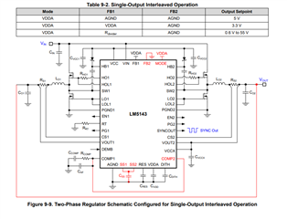
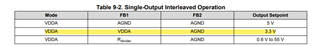
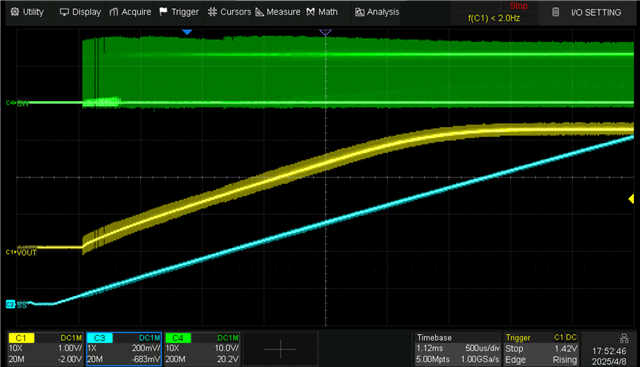
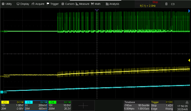
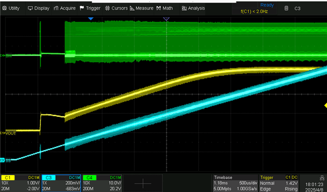
I'm going to use LM5143 to generate single output (10Vin to 3.3V @ 30A). Is this buck controller can be use for single output? If yes, Can you share any reference.
Tool/software:
Hi,
I'm going to use LM5143 to generate single output (10Vin to 3.3V @ 30A). Is this buck controller can be use for single output? If yes, Can you share any reference.