Tool/software:
Hi,
We are currently investigating an issue related to oscillation stop behavior in the UCC28740.
Although the exact root cause has not yet been identified, we have observed the following phenomena in the customer’s actual circuit:
-
A large ringing occurs on the bias winding voltage immediately when the FET turns ON.
-
This ringing may cause false detection on the CS voltage, which leads to the DRV signal being turned OFF within approximately 255ns.
-
This behavior is always observed immediately before oscillation stops.
-
The ringing continues superimposed until the auxiliary winding voltage reaches +20V, with a ringing frequency of approximately 12MHz, and takes about 1μs to settle.
-
At this point, we suspect that this ringing is primarily caused by the transformer design.
Based on the above, we kindly request your confirmation and response to the following questions:
Q1.
Please clarify the exact timing of the I_VSL data latch.
For example: Is the CS voltage latched A [ns] after the DRV signal turns ON?
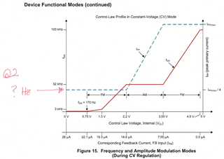
Q2.
On page 16 of the datasheet (CV mode operation), please indicate the switching frequency (fsw) when the peak current Ipp equals 1/4 of the maximum Ipp.
Q3.
In application note SLUAAC5, the following statement is made:
The Vaux ringing in Figure 8-1 is excessive and rings down below ground during tLK_RESET.
This behavior is known to trigger a UVLO fault and shut down the converter.
This is because when the VS pin crosses ground it activates input UVLO fault.
Does this mean that if the bias winding voltage undershoots below GND during the tLK_RESET period (when DRV is OFF), it can immediately trigger a false UVLO fault? Please confirm.
Q4.
Regarding Equation (24) in SLUAAC5, can the described fsw(max) be interpreted as the actual maximum switching frequency in CV mode during operation?
The maximum switching frequency observed in the customer’s circuit is approximately 70kHz.
This matter is time-sensitive. If a complete response is not immediately available, we would greatly appreciate it if you could provide us with an estimated timeframe for your reply.
Thank you very much for your kind support and cooperation.
Best regards,
Conor