This thread has been locked.

If you have a related question, please click the "Ask a related question" button in the top right corner. The newly created question will be automatically linked to this question.

TPS62933: Negative overshoot surpassing aboslute maximum rating

Part Number: TPS62933


Tool/software:

Hello,

I am currently using the DCDC controller to implement a buck covnerter 24/5V. I am validating the desing and I was taking a look at the overshoots in the switching node to make sure I am not exceeding the maximum aboslute ratings. The rating specfied of the switching node pin in the datasheet is -3V and 33V for 100ns. However in my case I have come accros the following issue:

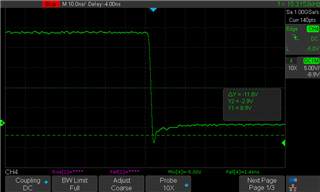
The turn off overshoot reaches -5V and a base value when on of  -500mV and the turn on is not in the image but I have measured about 500mV

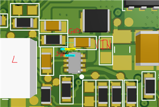
The measure is done by using the oscilloscope Teledyne T3DSO124 of 200MHz BW and 1GSa/s, the probe used is a probe CAT 2 with 200MHz BW. I am measuring the following points as shown in the PCB:

I am measuring using the GND in the closest decoupling input capactior and I am measuring directly in the SW pin. I am wondering why the turn off overshoot is perfect(Around 500mV overshoot and 24V input) but the turn on Overshooot reaches -5V. Furthermore, I though the IC would have already blown regarding that is surpasses quite a lot the recommended operating conditions and I am wondering If you could help me with this issue. I would like to understand where this overshoot comes from and what is done worng in the design, Also, I would like to know if I should except the IC to break soon.

Regards,

David

  • Hi David 

    Seems one of your image collapsed, can you attach it again. 

    Did you measure the SW-GND voltage using small-loop method? And please prove as close as possible to IC SW and GND pins. 

    I am wondering why the turn off overshoot is perfect(Around 500mV overshoot and 24V input) but the turn on Overshooot reaches -5V. ----Sorry I didn't understand, by turn on/off , do you mean the High side switch turn on/off. But the negative pulse you attached happens when SW down, which is HS turn off?

    I think the IC should have no risk to damage because of this, and can you please prove near the SW and GND pins and please use the smallest probe loop.

    Thanks and best regards.

  • Hello Gui,

    UI apologize, it seems that the image was not upload correctly, let me add it again. I am measuring the following points as shown in the PCB:

    Also, let me clarify the graph, I was referrring that in the turn off in low side, the overshooot was totally acceptable in turn off but the turn on was provoking issues as shown in the oscillocope image, where it can reach up to -5V.

    Finally, I am already using the pigtail method and proving as shown in the PCb image. I would like to know if that even though i am sunig pigtail the probing is not correct or is it totally possible having theses overshoting values.

    Regards,

    David

  • Hi David,

    The undershoot is a combination of two factors- first the break before make or dead time, which is in design to prevent any inrush current during the switching and the probe inductance. During the dead time the body diode of the low side FET conducts which causes voltage on LX node to drop, which may drop further because of the probe inductance. Now the value of current flowing through the inductor is higher when the high side switch turn off compared to when it turns on, hence the undershoot caused by the inductance is expected to be more than the overshoot caused while turn ON. 

    In longer run, this should not impact the device as this is expected and it is designed for the same.

    Regards,

    Himanshu