This thread has been locked.

If you have a related question, please click the "Ask a related question" button in the top right corner. The newly created question will be automatically linked to this question.

TLV1117: IDCY

Part Number: TLV1117
Other Parts Discussed in Thread: LM1117

Tool/software:

Hi,

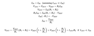
I'm working on a design where I use a couple of TLV1117 ICs in the adjustable version, and while looking at the datasheet, I noticed that the output voltage formula seems odd. It looks like the resistors R1 and R2 in the image (extracted from the datasheet) are inverted. Shouldn't R1 be above R2 instead of R2 above R1? An image of the typical application, extracted from the datasheet, is also included.

Best,
Rubén.

  • Hi Rubén,

    You're partially correct, it is inverted from most of our other LDOs. This is because the TLV1117 uses a floating topology unlike most of our LDOs. Essentially the device tries to reach a consistent voltage difference between ADJ and OUT while non-floating LDOs target a consistent voltage difference between FB and GND (Note that FB and ADJ have roughly analogous functions). This is why the resistor locations seem swapped.

    For ideal modeling, see the below equations (these should be satisfied when the device is properly regulating):

    Floating Non-Floating
    VADJ=VOUT-VREF VFB=VREF

    The TLV1117 uses a floating topology because it's a successor chip to the LM1117 which also used it.

    A quick derivation just to confirm, assuming IADJ is sufficiently small, per the datasheet (R1 & R2 should be calibrated to ensure this as well):

    IR2 is the current flowing from the VADJ node to ground through R2

    The equation is correct for this specific architecture.

    Best,

    Gregory Thompson