This thread has been locked.

If you have a related question, please click the "Ask a related question" button in the top right corner. The newly created question will be automatically linked to this question.

TPS7A57: Parallel LDO application schematic review

Part Number: TPS7A57

Tool/software:

HI, 

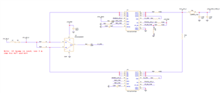
Based on the previous discussion, I have connected two TPS7A5701RTER is parallel as shown below. I am using Opamp just as optional circuit. This part of the circuit is kept DNP.

Request you to review and give feedback. I have some specific queries related to this circuit.

> Whether bias, PGOOD and CP_EN pins can be shorted between two LDO's?

> What is the purpose of Ballast resistor (R34 and R26)? If they are used for sensing current, whether sense pin should be connected after ballast resistor ? 

Thanks

Bharati

  • Hi Bharati,

    Yes - The bias, PGOOD and CP_EN pins can be shorted between both LDO's.

    A ballast resistor is an electrical component used to prevent current faults in a system. For parallel LDO designs it is placed between separate LDO outputs, and also between the  LDO output and the load. This limits the current that a single LDO can provide to the load.  Please see this collateral for further details:

    Parallel LDO Collateral:

    Parallel LDO Calculator

    13.5A low-noise high-accuracy LDO Reference Design

    Parallel LDO Architecture Design Using Ballast Resistors

    Comprehensive Analysis and Universal Equations for Parallel LDO's Using Ballast Resistors

    Thanks,

    Stephen

  • Thanks Stephen. This is helpful

  • Hi Stephen,

    Another question related to this regulator.

    We need all together 6A of supply at the load from both LDO's. 

    Do we see transients at output voltage due to this step load? Can you suggest, how this can be taken care in design?

    Thanks

    Bharati

  • Hi Bharati,

    FYI - you will want a local output capacitor between the LDO and the ballast resistors. You can copy C239 between U1 and R34 and also copy C239 to place between U3 and R26.

    What's the ramp rate of the load step?  What load is being stepped (is it 0A - 6A or something else)?  If the load step is slow enough then you will not see a transient as much as just load regulation.  To minimize load regulation and load transients, place the LDO's as close to the ballast resistors as possible (similar to the TPS7A57EVM-081 reference design) and place this parallel LDO circuit as close as possible to the load.  Make sure your sense lines are kelvin connected to the ballast resistor pad that is closest to the OUT pin of the LDO it is connected to.

    FYI - I realize the op-amp circuit is not populated, but if you were to ever use this you would want at least a capacitor from -IN to OUT (pin 1 to pin 4).  The value is probably small, around 1-10nF, so your case size can also be small (possibly an 0402 or 0201).  We don't have any hardware with this op-amp circuit used with the TPS7A57 so we cannot give any definitive guidance on how this performs or what values to use, but this is based on my experience with this method of parallel LDO designs.

    Thanks,

    Stephen