


Tool/software:
Hello,
We are using the BQ25171 to charge a single cell Li-ion battery when our system is connected to an external power source. We have also implemented a power path design similar to what is shown on page 29 of the datasheet. After experiencing a number of failures related to the charger circuit, we noticed that VIN = VBat - 0.7V during the off state. This is also causing functionality issues with our power path because VGS on the P-channel MOSFET is too low to reliably turn on. As a result, the system load power flows through the P-MOS body diode, resulting in a problematic voltage drop when the battery is not fully charged. We presume that due to /CE being 0V when power is off, one of the back-to-back switches in the BQ25171 is on, allowing current to flow through the body diode of the other internal switch and appear at VIN. 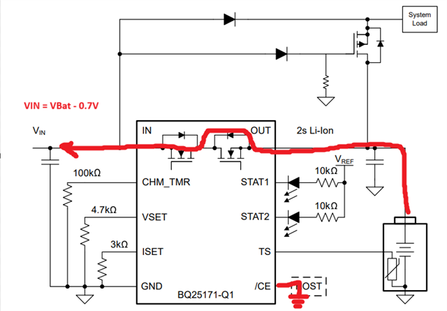
I have not been able to find information explaining how the device operates when VIN is not actively powered and /CE is low. Can someone confirm that this is what we are experiencing? Does /CE need to be pulled high at all times, even when power is turned off, to prevent leakage from the battery into VIN?
Thanks!
