This thread has been locked.

If you have a related question, please click the "Ask a related question" button in the top right corner. The newly created question will be automatically linked to this question.

TPS40305: TPS40305 Failure after several seconds/ minutes of running?

Part Number: TPS40305
Other Parts Discussed in Thread: CSD18543Q3A

Tool/software:

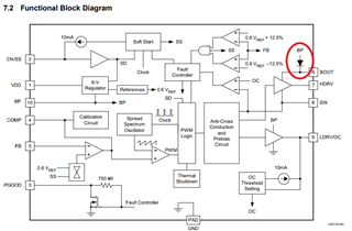
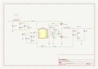
I'm currently working on a USB hub that utilizes a TPS40305 to regulate the 5V bus voltage from a 12V input. I got the design from WEBENCH, with an IOUT Nominal of 10A. The main modification I made was using PGOOD to enable a 3.3V LDO for the hub IC, however looking back at my design, it also looks like the FETs are slightly different (looking around at other designs on the forum I'm seeing issues with high gate capacitance and this controller.

After running for a few minutes with a 2A load, the output shuts off, and it seems like the controller can't initialize. EN ramps up repeatedly, and the feedback pin just has an occasional "blip". Can anyone point me towards what might be happening here? I'm having difficulty recovering boards by resoldering the 40305, and I'm not sure what I should be looking for to pin down and eliminate this issue

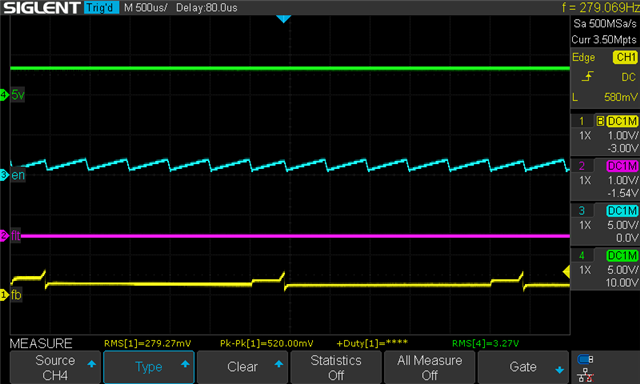
Just to add- I removed the output to confirm that the issue wasn't load related, and the behavior persists

  • Hello, 

    Please make sure you have enough COUT, just looking at the design, i see that COUT is only 10uF. please use at least 3X that much. 

    I can not tell what is the Inductor used in the you circuit, but around 820nH is needed. 

    Lastly, for the COMP, please use Comp of 8.2nF and R comp of 1.65K

    Thanks!

    Tahar

  •  

    Here is the link for the design tools for the TPS40405 controller to help with the compensation design : https://www.ti.com/product/TPS40305#design-tools-simulation 

    https://www.ti.com/tool/download/SLUC263 

    The Sumida inductor looks like its 1.2μH.  For 12V to 5V @ 1.2MHz, that's about 2A of peak to peak ripple, which should be ok.

    I the 11nC gate charge of the CSD18543Q3A will require are 13mA of current to drive the high-side FET at 1.2MHz, which could be a factor, it's possible that the 13mA of current has fused metal in series with the BP to BOOT diode.  You could confirm that is the issue by applying an external diode from the BP bypass capacitor to the BOOT capacitor.

    You can also monitor the BOOT, and HDRV signals on an oscillscope at the switching frequency to confirm BOOT is not regarding to the BP voltage when the switch node is low, and boot-strapping to VIN + BP when the switch node is high.  The Switch Node will also not rise to VIN without power at the BOOT pin.

    Rather than using a 60V MOSFET with a 20V rated gate drive, you could get a similar Rdson (9.9mΩ) with a lot less gate charge selecting a 30V MOSFET For example - https://www.ti.com/lit/ds/symlink/csd17579q3a.pdf a 30V MOSEFT with similar Rdson and half the gate charge.

    If waveforms show that the BP to BOOT diode is working, and the converter is still shutting down, as can check the compensation using the SLUC263 spreadsheet and check the stability.

  • Thank you - I have a 56uF directly on the output, and each power switch for USB output has 56uF as well.

    The inductor is a Sumida 0630CDMCDDS-1R2MC with 1.2uH, so that should be OK

    Could you elaborate on your suggestions for the compensation components?

  • Thank you for the advice and link to the compensation tool! I look forward to trying it.

    Just to make sure I understand, is the hypothesis that the diode between BP and BOOT has failed, so an external one should allow it to work? Do I need a specific type, or will generic be acceptable?


    I'll check the BOOT and HDRV signals on the scope and report back

  •  

    Thank you - I have a 56uF directly on the output, and each power switch for USB output has 56uF as well.

    Do you have the specifics of the 56μF capacitor(s) on the and each USB switch?  How many total USB switches are there?

    Could you elaborate on your suggestions for the compensation components?

    We can enter the total capacitance and ESRs into the https://www.ti.com/tool/download/SLUC263 excel spread sheet and evaluate the loop, and any potential changes.

    Just to make sure I understand, is the hypothesis that the diode between BP and BOOT has failed, so an external one should allow it to work? Do I need a specific type, or will generic be acceptable?

    It doesn't need to be a specific type.  It needs to be able to handle more than 13mA of average forward current with much higher peak currents, I would look for a peak current greater than 1A due to the recharging current for the boot-strap capacitor.

    It needs to withstand a reverse bias at least equal the peak switch node voltage minus the BP voltage.  Generally I would recommend a 25-30V diode

    Most designs would use a low forward drop shockley diode, but a standard silicon rectifier diode will work as well.  Typically, by the end of the low-side FET on-time, the BP to BOOT current through the diode has dropped to near zero, do the forward drop of the diode isn't typically important.

  • Adding an external diode worked - thank you!!

  • Glad to be able to help you.