This thread has been locked.

If you have a related question, please click the "Ask a related question" button in the top right corner. The newly created question will be automatically linked to this question.

LM5190: PCB layout help

Part Number: LM5190

Tool/software:

Howdy,

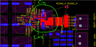
On a previous post I asked some question on the layout of 48V to 5V (17A output) buck converter using the LM5190 chip. Attached is a picture of PCB with some preliminary placements of components, without tracing completed. I once again have questions pertaining to creating a PCB similar to the EVM:

1. The data sheet in 7.4.1.1 mentions that for loop 1 "connect the input capacitor or capacitors negative terminal close to the source of the low-side MOSFET. Similarly, connect the input capacitor or capacitors positive terminal close to the drain of the high-side MOSFET." Since I have a large, beefy input capacitor to connect there, I found that placing it on the bottom side of the PCB would meet those requirements. I attached a picture (but if needed I can send files) to show this: there is one input capacitor to the left of the FETs, and another one at the bottom of the FETs. Is it reasonable to use this configuration? Does tracing loop 1 through the bottom plane cause issues? Might it interfere with the input filter I have placed somewhat near it?

2. I looked at the EVM and I notice there are a lot of vias to place. Is there a script that TI uses to generate all the vias that connect the planes? That would be helpful.

Thanks,

Yoav Binyamin,

Texas A&M University

  • Hello Yoav

    SMD ceramic input capacitors should be placed closed to the IC on the top layer. 

    Leaded aluminum capacitor can be placed on the bottom side of the PCB (assuming the IC is placed on the top side of the PCB), but also you have to make sure a large ground copper is connected to the DAP/EP vias on the bottom layer for a thermal dissipation.  

    Input filter should be located close to the input terminal, away from the SW node. 

    The ground vias were placed using the 'Via Stitching/Shielding' function of the Altium tool. 

    -EL 

  • Thanks; I will keep the input capacitors as is, and I was planning to place vias in pad on EP. For context this will be a 4 layer board, and that large Cin input capacitor should not interfere too much with the chip's ground connection.

    For that input filter, can you elaborate on "away from the SW node?" Can the filter be placed on the layer below the chip at all, or not? Do you recommend moving the input from the right to the left and moving those filter capacitors on the left away from the chip (possibly downwards)? Must the filter be placed spatially between the input voltage and the connection to the chip and power components?

    -yb

  • Hello Yoab 

    Filter can be placed on the bottom layer below the IC. Please use the inner ground layer as a shield.  

    Input filter means input LC filter.  The LC filter should be located away from the switching node which is noise source. 

    -EL