This thread has been locked.

If you have a related question, please click the "Ask a related question" button in the top right corner. The newly created question will be automatically linked to this question.

LM51561H: How to reduce strong EMI disturbances

Part Number: LM51561H

Tool/software:

Hello, 

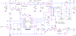
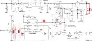
we have implemented a regulator with your component in SEPIC mode to produce an output of 110V, with a wide range input of 16.8V to 137.5 V.

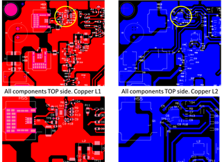
The proto is working, but EMI disturbances are very high, due to LM51561H behavior and its circuitry. We need to lower at 15-20dB to comply to railways standards.

  • Hi Silvana,

    Thanks for using the E2E forum.

    Can you please share the SW node signal waveform for the converter at full load?

    Best Regards,

    Hassan  

  • The blue channel is the signal at pin 4 LM51561H , when supplied with 30V

  • Hi Silvana,

    Thanks for sharing the scope plots.

    As I see a ringing on both rising and falling edge of your SW node, can you please measure the ringing frequency at the SW node? 

    And can you please confirm that the ringing frequency at the SW node is the same frequency at which you fail the EMI test?

    If yes, then I would recommend to optimize the speed of your FET by adding the gate resistance at the gate signal of the FET or by adding the snubber circuit between SW to ground. 

    Moreover, I recommend to add 100ohms R5 resistor. It helps to filter out the high frequency noise in your current sense signal.

    Best Regards,

    Hassan 

  • Hello Hassan,  

    unfortunately the disturbances are in a wide frequency band. The result at 24V supply, horizontal 30MHzto1GHz follows:

    We have actually tried adding the gate resistance: in order to comply with the standard we had to use a 100R, but we noticed some heating in the circuit.

    We have also changed R5 to 4K7 and all the red components in the following schematic.

    With the modified circuit the we could only lower the EMI at 24V, but couldn't solve it up to 110V supply, which is our upper limit.

  • Hi Silvana,

    Thanks for sharing the EMI result.

    As per the results, it is clear that spectrum of frequencies causing the issue.

    Firstly, I would not recommend to use gate resistance more than 10ohms because it will cause a lot more switching losses. I recommend to add parallel gate to source capacitance to Low side FET to reduce the switching speed. 

    Moreover, are you using shielded inductors in your design?

    Additionally, the PCB parasitic would also cause this EMI issue. Because fast di/dt would cause high voltage spikes at power loop parasitic inductors, which would be a source of EMI. 

    Can you please share your layout files?

    Best Regards,

    Hassan 

  • Hello Hassan, 

    yes we are using shielded inductor COILCRAFT MSD1514-104KED in L1 position.

    The board has a double layer PCB. Please find the details below.

    Thanks and Regards,

    Silvana

  • Hi Silvana,

    It is a public holiday till next Monday. Please expect a reply by next Tuesday.

    Best Regards,

    Feng

  • Hi Silvana,

    I have gone through your layout and found that you have a very large switch node area. Large switch node area is a major source of EMI because of discontinuous current. 

    I would recommend to optimize this area and try to reduce the switching speed of the FET by adding a gate to source capacitor to it. 

    Best Regards,

    Hassan

  • Thank you, Hassan, for your analysis.

    We were, in fact, very doubtful about the layout.

    1.Do you also suggest to increase the number of layer to add some GND planes inside?

    About the architecture, from first image of the schematic, you can see we have not included a proper common mode filter at input stage neither we have predisposed a RC filter connecting GND to EARTH (at the moment GND is floating).

    2. Do you recommend adding those filters?

  • Hi Silvana,

    Yes, I would suggest to use 4 layer PCB. With top land bottom layers for power routing. Try to place current going path top of the current return paths. In this way the power loop parasitic inductance will minimize because of magnetic field cancelation.  

    Try to add ground planes around the power loop at top layer, it will also provide the magnetic field cancelation. 

    Try to use third and forth layer for signal routing. With analog ground on third layer and signals at bottom layer. 

    Yes, you have not use the decoupling caps at the input and output. Try to add multiple decoupling caps at input and output (100nF).

    Try to reduce the gate loop area because this can also be a source of EMI. Try to make a short connection to the gate. Going and return path for the gate signal should be place close to each other or overlap each other if you are using the two layers for gate signal. 

    Apart from this, add snubber circuit at the SW node. Try to use Power stage designer to calculate the RC snubber network values for Sepic.. 

    https://www.ti.com/tool/POWERSTAGE-DESIGNER?utm_source=google&utm_medium=cpc&utm_campaign=app-gen-null-163201522726_powerstage_designer_rsa-cpc-evm-google-eu_en_int&utm_content=powerstage_designer&ds_k=power+stage+designer&gad_source=1&gbraid=0AAAAAC068F27xAYE4NUcsOekY99VseYGS&gclid=CjwKCAjwn6LABhBSEiwAsNJrjtfx6hcnqTnPdUZyf8q8rLlkTlq9VJ2DA05oh05GqdgzRGCh-Vit0BoCJEIQAvD_BwE&gclsrc=aw.ds

    Connect the PGND with the AGND with one tie connection.

    Yes, if it is not battery driven device, then you can add a filter to connect GND to Earth. It will also provide a ESD protection to the device. 

    Best Regards,

    Hassan