This thread has been locked.

If you have a related question, please click the "Ask a related question" button in the top right corner. The newly created question will be automatically linked to this question.

UCC21551: Technical Inquiry on UCC21551: Cost Structure, High-Frequency Reliability, and Fault Modes

Guru 12020 points
Part Number: UCC21551
Other Parts Discussed in Thread: UCC21520

Tool/software:

Hi,

We would like to inquire about the following three technical topics regarding the UCC21551 isolated gate driver:

The UCC21551 is offered at a significantly lower price point compared to other 2-channel reinforced isolation gate drivers from TI (e.g., UCC21520).
We assume that this cost difference may be due to differences in feature set, internal architecture, isolation specifications, or manufacturing process.
Could you please clarify the main technical or design trade-offs that contribute to this lower cost?

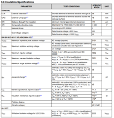
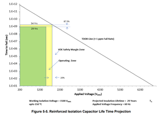
In applications where commercial AC line-related noise (e.g., 50Hz or 60Hz waveform leakage or AC ripple voltage) is continuously coupled to the high-side terminal of the isolated gate driver,
is there any concern regarding long-term reliability, degradation, or abnormal behavior due to stress on the internal isolation barrier or output stage?
Specifically, if such low-frequency AC noise is superimposed across the isolation barrier for extended durations, could this affect insulation lifetime or functional stability?
If any internal evaluations or design guidance exist related to this use case, we would appreciate it if you could share those details.

In a half-bridge configuration, if both high-side and low-side FETs are accidentally turned on simultaneously (i.e., shoot-through condition),
what kind of failure modes are expected within the isolated gate driver?
We are particularly interested in potential damage mechanisms at the output stage, breakdown of internal circuits, or insulation failure under such stress.
Any known failure analysis or test results under this condition would be appreciated.

Best regards,

Conor

  • Hi Conor,

    Thank you for your interest in our devices and reaching out to us with these questions.

    1.) UCC21551 uses the latest TI ISO process and is created using a larger wafer (200mm in 21520 to 300mm in UCC21551). This combined with a smaller die design, the cost structure between UCC21520 and UCC21551 has improved significantly. With this in mind, the purpose of releasing UCC21551 was to address many of the common failure modes seen in UCC21520 and ultimately create a more robust version. I would highly recommend to consider UCC21551 over UCC21520 for these reasons.

    2.) These isolated gate drivers are made to operate in high voltage/power systems where noise transients are expected. The insulation specifications in the product's datasheet (see snippet below) is a good reference to see what kind of conditions this driver is able to withstand. 

    3.) UCC21551 does not have any fault detection or current protection feature like some our single channel isolation gate drivers have, so this would have to be implemented externally. However with the interlock function enabled on UCC21551 along with proper schematic and layout guidelines, there should not be a case where both FETs turn on simultaneously.

    Hope this helps. Please feel free to ask any additional questions below.

    Regards,

    Hiroki

  • Hi Hiroki,

    Thanks for your reply.

    2.) These isolated gate drivers are made to operate in high voltage/power systems where noise transients are expected. The insulation specifications in the product's datasheet (see snippet below) is a good reference to see what kind of conditions this driver is able to withstand. 

    We already know that the datasheet defines the isolation specifications based on IEC standards, i.e. how much noise the IC can handle. What we want to know is whether the TI provides any information about long-term reliability (lifetime of the IC) in applications where commercial AC line-related noise is continuously applied to the high-side terminal.

    3.) UCC21551 does not have any fault detection or current protection feature like some our single channel isolation gate drivers have, so this would have to be implemented externally. However with the interlock function enabled on UCC21551 along with proper schematic and layout guidelines, there should not be a case where both FETs turn on simultaneously.

    You are correct that it is necessary to design so that both FETs are not turned on at the same time. However, in isolated applications, "unexpected and unintended behavior" must be considered. Is any information provided about failure modes if both high-side and low-side FETs are accidentally turned on at the same time?

    Thanks,

    Conor

  • Hi Conor,

    Is the TDDB curve sufficient enough to address your concerns? 

    For more information, see https://www.ti.com/lit/ml/slyy191/slyy191.pdf 

    Is any information provided about failure modes if both high-side and low-side FETs are accidentally turned on at the same time?

    What specific information would be helpful? Typically when both high-side and low-side FETs are turned on at the same time in a system, it is difficult to pinpoint the root cause to be a failure in the FETs or the gate driver. Voltage or current transients can cause failures in the FET component but also could cause accidental turn on in the gate driver due to Miller charge injection.

    Miller induced turn on can be avoided by minimizing the gate loop inductance and adding a 10kohm pull down resistor at the gate of the FET to the source. Other methods such as Miller clamps can be implemented to further prevent this from occurring 

    Here is more information on Miller clamps: https://www.ti.com/lit/ab/slya091/slya091.pdf?ts=1744656496204&ref_url=https%253A%252F%252Fwww.google.com%252F 

    Hope this helps. Feel free to ask any additional questions below.

    Regards,

    Hiroki