Tool/software:
Hi guys,
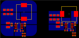
I've attached two different layouts for LMR38020 at 3.3V 0.5A output
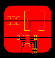
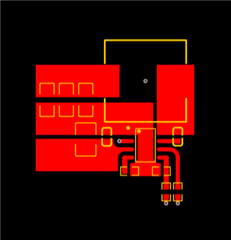
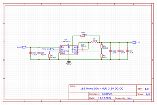
If i reduce the width of the switching track in design 1, can it be used ?
The test pcb will be 4 layers - 2oz / 1oz / 1oz / 2oz - The inner layers will be GND and 3.3V
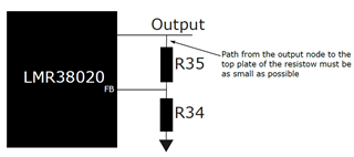
do let me know if any other changes are recommended
Thanks & Regards,
Muki