This thread has been locked.

If you have a related question, please click the "Ask a related question" button in the top right corner. The newly created question will be automatically linked to this question.

TLVM23615: PCB issue for TLVM23615

Part Number: TLVM23615
Other Parts Discussed in Thread: LMQ66430,

Tool/software:

Hello,
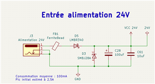
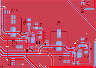
I'm having a problem with the TLVM 23615.
I use this component to convert 24V to 5V and 3.3V to power CPUs.
For 3 out of 5 boards I've had built don't work.
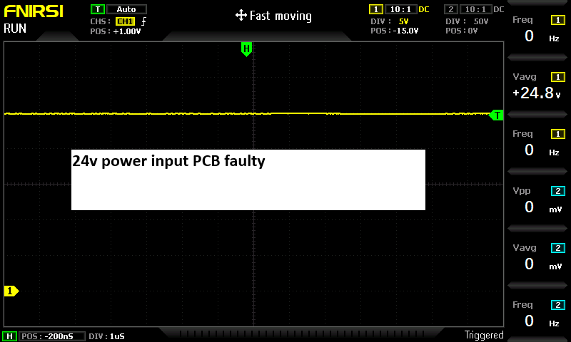
24V arrives correctly on VIN and EN, but the output voltage is 0.
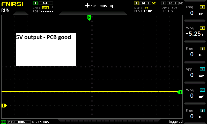
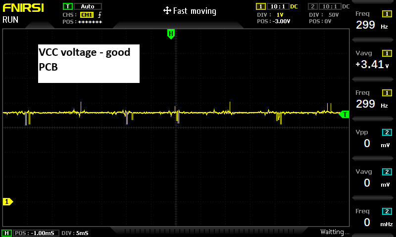
On 2 boards that work well, the output voltage is correct.
The schematic was designed by TI's tools.
So, it's a problem with the PCB design or the track layout, but I don't understand why.
Please help me. Any advice accepted!

  • Hi, 

    Can you swap out the working ICs to the non-working boards? This will tell us if it's an IC issue or a board issue. Please carefully label the ICs and the boards and take note of which combinations are working. 

    Regards,

    Rahil

  • I can't change the components. All 5 boards were manufactured by the same supplier (JLCPCB) with the same components. They are on the main board. They can't be removed. I suspect a ground or insulation fault on the pins under the bucks, but I can't investigate that. This is why I sent you the PCB plan in the 1st message made with KICAD to see if the footprints are correctly respected, particularly at the GND level.

  • Hi Oliver, 

    If the footprint was the problem, none of the boards would work. Could you make sure the IC orientation is the same on all the boards?

    Once you confirm that, please take some scope shots for me of EN, SW and VCC on the good and bad boards. 

    Regards,

    Rahil 

  • Thank you Rahil.

    I checked the components; they're all correctly oriented. These are factory-made PCBs. I'll do the oscilloscope analysis tomorrow evening (Paris time).

    Here is the electrical diagram for 24v from a 75w adapter.

    Thank you very much for your help.

  • Sounds good. You can post the pictures on here when you get them.

    Regards,

    Rahil

  • Hello Rahil,

    Here are the images taken with my oscilloscope between a working board and a non-working board.

    For each board, I've attached:
    Voltage at the power connector (24V) 
    Output voltage of the 16V circuit based on an LMQ66430. This output works on all my PCBs (5/5)
    Voltage at the EN pin of the TLVM23615 -> 24V on 5/5 PCBs
    Voltage at the SW -> big difference between a working PCB and a non-working PCB!
    Output voltage of the 5V (3/5) PCB doesn't work.
    I hope you can help me find the problem.
    Sincerely,
    Olivier

  • Hi Oliver,

    So the bad boards are not switching at all. Could you also send me screen captures of VCC and FB? 

    Regards,

    Rahil

  • Does the SW,FB and VCC voltage on the good circuit seem correct to you?
    Here are the FB and VCC outputs on the two good and bad PCBs.

    For the BAD -> All signals are 0V

    Regards,

    Olivier

  • Hi Oliver,

    I suspect there is something wrong with the ICs. My best guess is that that ICs were somehow damaged. 

    Regards,

    Rahil

  • Since there are a lot of capacitors, there is a spark when I connect the power supply.

    I will modify this point with a MOSFET-P to have a soft start.

    Do you think the origin comes from there or from defective components or even a manufacturing problem?

  • It is possible but since the EN and Vin going into the IC is high, it makes me thinkl the IC is the problem. 

  • Thank you for your help.

    I'm going to have new boards made with these components to test other modifications.

    I'll let you know the results in about a month.

  • Hi Oliver,

    In the new boards, if you're changing layout - I recommend following layout guidelines in the datasheet.

    Regards,

    Rahil

  • Hi Rahil,

    Here is my new layout.

    I've tried to do my best reading the datasheet.

    I hope it will works now. I will keep you informed.

  • Hi Oliver,

    Looks better. Additional tips from datasheet that might be helpful:

    1. Place the input capacitors as close as possible to the VIN and GND terminals. VIN and GND pins are adjacent, simplifying the input capacitor placement.

    2. Place bypass capacitor for VCC close to the VCC pin. This capacitor must be placed close to the device and routed with short, wide traces to the VCC and GND pins.

    3. Place the feedback divider as close as possible to the FB pin of the device. Place RFBB, RFBT, and CFF, if used, physically close to the device. The connections to FB and GND must be short and close to those pins on the device. The connection to VOUT can be somewhat longer. However, the latter trace must not be routed near any noise source (such as the SW node) that can capacitively couple into the feedback path of the regulator.

    4. Use at least one ground plane in one of the middle layers. This plane acts as a noise shield and as a heat dissipation path.

    5. Provide wide paths for VIN, VOUT, and GND. Making these paths as wide and direct as possible reduces any voltage drops on the input or output paths of the power module and maximizes efficiency.

    6. Provide enough PCB area for proper heat-sinking. Sufficient amount of copper area must be used to ensure a low RθJA, commensurate with the maximum load current and ambient temperature. The top and bottom PCB layers must be made with two ounce copper and no less than one ounce. If the PCB design uses multiple copper layers (recommended), these thermal vias can also be connected to the inner layer heat-spreading ground planes.

    7. Use multiple vias to connect the power planes to internal layers.

    Let me know if there is still a problem.

    Regards,

    Rahil

  • Hello,
    I'm delighted to see that my 5 new PCB i have received today are 100% functional in terms of power supply with the TLVM23615s.
    The two main changes are:
          Removal of the external connection between the two SW pins (although the TI design software displayed it on the schematic)
          Improved isolation design (increased the isolation of unused pins, including the two SW pins).

    Thank you for your help. This solves my problem.

  • Hi Oliver,

    Glad to see your problem is solved. Closing this thread, please start a new one if you need any further help.

    Regards,

    Rahil