Other Parts Discussed in Thread: TPS1HTC30-Q1,
Tool/software:
Dear Sir/Madam,
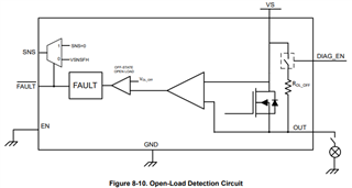
I'm evaluating the TPS1HTC30-Q1 part on the TPS1HTC30EVM board, and I'm seeing very strange behavior. J3 is the 3-pin header where the EN pin can be connected to 3.3V or GND. I have the 3.3V LDO enabled on this EVM, and I've confirmed that I'm getting 3.3V. When I jumper EN to GND, it's supposed to turn off the high side switch. If I have no load on the output, the input voltage on J11 shows up on J13, regardless of the EN pin connection. If I put a small load (10k on 14V, drawing 1.4mA), then the EN pin does switch the output, but only down to 1.04V. Our application requires the output to be at (or very close to) 0V when the high side switch is disabled. I didn't see a minimum load requirement in the datasheet. Could you elaborate, so that I can design this part in with enough margin for production? I can put a nominal load on the output to make sure the output does stay at 0V, but I would want to know what's going on in the IC, and make sure the load I have on it will guarantee the output will be 0V.
In addition, we're using this in a 48V system. I understand the TPS1HTC30-Q1 is good to 60V, but the TPS1HTC30EVM specifies the max voltage to be 48V. What's the limitation for the TPS1HTC30EVM that caps the voltage at 48V?
Thanks and best regards,
Kent