Other Parts Discussed in Thread: LM25141, LM5141-Q1,
Tool/software:
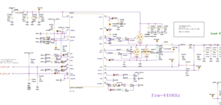
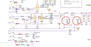
How to measure the Bode of LM25141? Where to inject interference signals? R3443 or R3444?
Tool/software:
How to measure the Bode of LM25141? Where to inject interference signals? R3443 or R3444?