This thread has been locked.

If you have a related question, please click the "Ask a related question" button in the top right corner. The newly created question will be automatically linked to this question.

LMG1210: Variable Inductor Buck Conveter Layout Review

Part Number: LMG1210

Tool/software:

Hi 

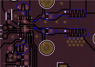
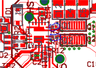
we are developing a GANFET based Buck converter using LMG1210 driver by following the LMG1210-EVM schematics and Layouts to Achieve optimal PCB inductance and less noise.

the Objective of the Board is to be Able to control the Buck Converter through a Raspberry Pi Pico PWM signals with  Choice of Different Inductors for Testing Purposes.

We would like You to Review Our Layout and Provide valuable Feedback and Recommendations.

Below attached link is the Kicad Canvas of our Project, the Github of the Project files is also attached below

https://kicanvas.org/?github=https%3A%2F%2Fgithub.com%2Fsuryathanush%2FGanFET-Buck-Converter

https://github.com/suryathanush/GanFET-Buck-Converter 

Please Review them and Give us your Feedback

Thank You
Surya Thanush

  • Hello Surya,

    The schematic looks good. Make sure to place the VDD bypass cap and HB-HS bootstrap cap as close to the driver as possible. The HO and LO output traces to the GaNFETS and gate resistors should be kept as short as possible.

    Please let me know if you have any other concerns.

    Thanks,

    Walter

  • Thanks Walter for the Schematic review,
    Can you also provide some feedback on our Layout. it was in the same folder.

    Thanks in Advance

    Surya Thanush

  • Hello Surya,

    The overall layout looks good but I would try and move capacitors C4 and C7 and the gate resistors R11 and R12 and the GaN FETs closer to the driver if possible. This will help reduce PCB parasitics on the critical traces

    In the EVM, the gate resistors are very small 0201 size to make the output traces as short as possible.

    Thanks,

    Walter

  • Hi Walter

    Thank you for your Review.

    we actually imported footprints of IC and Feed-through capacitors from Samcsys (https://componentsearchengine.com/), which was recommended by Mouser and Arrow electronics for ECAD files.

    Those imported footprints have larger Courtyards, so the colses we could get with C4, C7 and driver is this.
    Below attached is the screen shot from the Kicad PCB showing the Courtyards.


    I believe this bigger Courtyards given by community is needed for ease of Assembly and Re-flow, not sure. so Kept them as it is.


    And regarding the Gate resistors, we intentionally had 0603 because it would be easy to swap them as per needed in the testing.
    If it's really critical for better Gate driving, we shall change them. need your verdict.

    Thank You
    Surya Thanush

  • Hello Surya,

    The current capacitor placement should be fine with the given layout courtyards. 0603 size is fine as well. A smaller size would allow the gate drive path to be made shorter but the current layout should be fine.

    Thanks,

    Walter

  • Oh, thanks for the Confirmation Walter.
    Your help is really appreciable