This thread has been locked.

If you have a related question, please click the "Ask a related question" button in the top right corner. The newly created question will be automatically linked to this question.

TPS23882B: TPS23882B1RTQR : Not Powering ON as expected

Part Number: TPS23882B

Tool/software:

Hi Team,

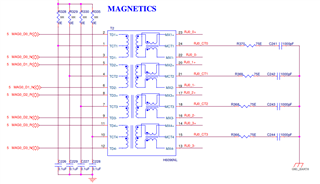
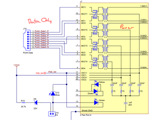
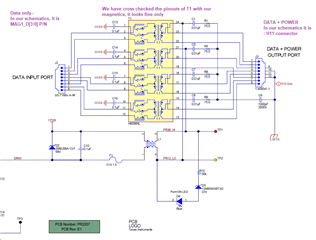
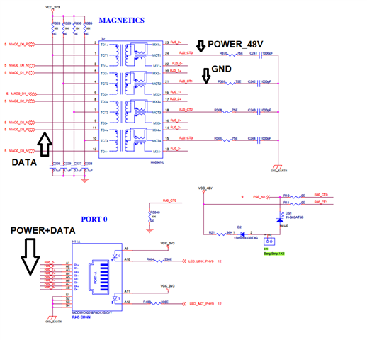
We are using TPS23882B1RTQR in our design for POE section.

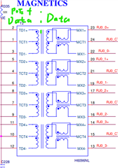
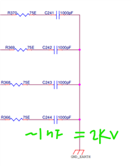
We have referred the  TPS23882EVM used guide and designed exactly as per the reference design. 

Please find the attached schematics for your reference.

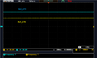
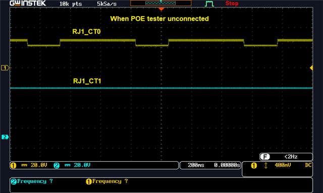
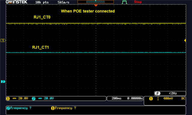
After power ON & connecting 48V, our observations as follows

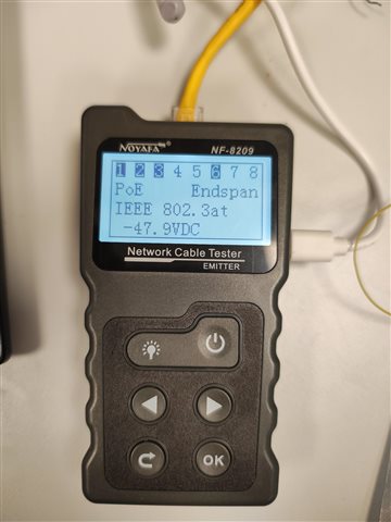
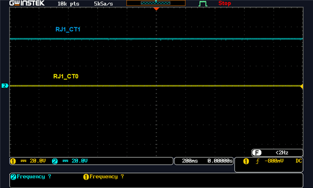
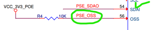
RJ1_CT1 : is  48V, which is OK.

AT RJ1_CT0 : We should get 0V after connecting properly, but we getting 22-27V. 

CH2_GATE : 0.4V, CH2_SEN : 0.4V, PSE_N2 is toggling from 22-27V. 

Please guide us.

Regards

GuruPDF-EPCB-9038-O-00_texas.pdf


  • Hi Guru,

    I will look into this and provide a response today. Thanks!

    Regards,

    Brandon

  • Hi Guru,

    When probing the port you should be probing between RJ1_CT0 and RJ1_CT1. This will be your differential, you should not probe these two signal between ground. 

    Also, from the schematic, looks like your magnetics or incorrectly wired. Your CMC of the ethernet magnetic should be on your data only side, not your power + data side which is what you currently have. 

    Regards,

    Brandon

  • Hi Sir,

    Sorry for the late reply. Due to some unavoidable situations, I am unable from my end.

    Regarding the query, please find the below image : 

    As per the reference J2, in our schematics it is from the MAG1_D[3:0]P/N

    MAGNETICS is placed correctly

    As per the reference J3, in our schematics it is H11

    Please find the schematics & image below.

    I shall also probe & update you at the earlier.

    Regards

    Guru

     7127.PDF-EPCB-9038-O-00_texas.pdf

  • Hi Guru,

    Please let me know the results with waveform captures when you are able to capture. 

    Regards,

    Brandon

  • Hi Sir,

    Sorry for the late reply. Please find our observations while probing RJ0_CT0 with RJ0_CT1

    We have connected 48V supply & shorted the 12V GND & 48V GND. In open condition, without connecting anything  we found this observation 

    Please find the below waveform.

    When we have connected the RJ45 with the POE tester, we found the following observation, 

    also in POE tester, we found the following image in POE Tester.

    Please guide us.

    Regards

    Guru

  • Hi Sir,

    Also, for debugging just to manually turning ON the mosfet or bypassing the mosfet, we got the following observation

    Rework done :  R12 directly connected to ground / shorted to ground. 

    Then we got the following observation.

    The circuit works as per our requirement. Require your support.

    Regards

    Guru 

  • Hi Guru,

    I have transitioned roles and have re-assigned this to one of our PoE experts to help resolve. 

    Regards,

    Brandon

  • Hi Guru,

    Please check below items and let me know if it is still not working. Thanks.

    1. The data transformer normally makes the PoE on the side without CM choke. Since the PoE current is CM. Please check with H6096NL vendor.


    2. Bob Smith terminal normally has a >2kV cap between earth GND


    3. /RESET better has a discharge loop. You may short D8.


    4. Please short the unused Kelvin sense to AGND


    5. You can leave OSS open (DNP R4) if you do not have a net connect to PSE_OSS

    Best regards,

    Diang

  • Hi Sir,

    1. The data transformer normally makes the PoE on the side without CM choke. Since the PoE current is CM. Please check with H6096NL vendor.

    We are communicating with the vendor. We shall update you at the earliest.

    2. Bob Smith terminal normally has a >2kV cap between earth GND

    We are using the 1210GC102KAT2A – 1000 pF ±10% 2000V (2kV) Ceramic Capacitor X7R 1210 capacitors at  C241, C242, C243, C244, C237, C238,  C239, C240

    3. /RESET better has a discharge loop. You may short D8.

    Rework done as per the suggestions.

    4. Please short the unused Kelvin sense to AGND

    As the component is QFN Package, we are unable to do it. Is there any alternative for that or is it mandatory to do the rework.

    5. You can leave OSS open (DNP R4) if you do not have a net connect to PSE_OSS

    Rework done as per the suggestions.

    Even after the reworks, the POE section is not working.

    Regards

    Guru

  • Hi Sir,

    1. The data transformer normally makes the PoE on the side without CM choke. Since the PoE current is CM. Please check with H6096NL vendor.

    H6096NL  supports  4PAIR PoE 75W

    Regards

    Guru

  • Hi Guru,

    Thanks for your reply. 

    1. It is not about the power rating of the data transformer. You may need to know which side (left or right) is for PoE + Data and which side is for Data only.  

    Can you get the waveforms of Q1 and Q2's Vds and Vgs when port is open and connected? It seems FETs behaviors are strange.

    Best regards,

    Diang 

  • Hi Sir,

    Please find the waveforms for Q2 for Vgs & Vds when connected & unconnected conditions.

    Vg_Vs when POE tester not connected.

    Vg_Vs when POE tester connected

    Vd_Vs When POE tester unconnected

    Vd_Vs when POE tester connected

    Also we are using the application as per the attached image

    Regards

    Guru

  • Hi Sir,

    Please ignore the earlier waveforms.

    In board we have GND & 48V_GND, The above waveforms are captured without shorting the grounds. Please find the waveforms with shorting the grounds.

    Vg_Vs When POE tester unconnected

    Vg_Vs When POE tester connected

    Vd_Vs When POE tester unconnected

    Vd_Vs When POE tester connected

    RJ1_CT0 & RJ1_CT1 When POE tester unconnected

    RJ1_CT0 & RJ1_CT1 When POE tester connected

    Regards

    Guru

  • Hi Guru,

    Thanks for your quick reply. I will get back to you by this week.

    Best regards,

    Diang 

  • Hi Sir,

    While our debugging, we observed the CDS16403 (Vds = 25V Max) part has been placed. 

    As per our circuit the Vds = 48V (Double to capacity of the MOSFET mounted), so we are considering this is the issue, Due to higher Vds, the MOSFET is damaged & Gate junction has been collapsed. So we are getting Vg=0V, Ve=0V. 

    We are proceeding for the new Gerber, for the safer side, we shall update it & share the schematics for your reference. Please review & share the feedback. 

    We shall share the updated schematics at the earliest.

    Regards

    Guru

  • Hi Guru, 

    I am out of office currently. Will get back to you later. Thanks for patience. 

    Best regards,

    Diang

  • Hi Guru, 

    Thanks for updates. Yes it makes sense that FET Vds rating is the cause of abnormal voltage at the port.

    Best regards,

    Diang

  • Hi Sir,

    Now we are removing the mounted FET Q1,Q2. And want to change the chipset from autonomous mode to I2C mode. Via I2C we want to manually enable the gate and want to check the voltage of Vg pin (in open condition at Vg pad) just to ensure in next revision it shall work properly and no other issues are there in the board. 

    So as per datasheet & schematics, we are using address 0X20. But still we are unable to detect the Chipset. Please support us, that what shall be the address for the CHISET. We have pulled LOW for A4,A3,A2,A1 pins as per the schematics.

    Regards

    Guru

  • Hi Sir,

    Please review the schematics and share the feedback.

    Regards

    GuruPOE_TEXAS.pdf

  • Hi Guru,

    Thanks for your updated schematic.

    We will get back to you in 2-5 business days. Thanks for your patience. 

    Best regards,

    Diang

  • Hi Guru,

    You should be able to use 0x20 slave address when A4-1 are ground. Do you have a Saleae waveform about the SDA and SCL at TPS23882B. Also, can you try if you can access the boardcast address?

    See the comments about the schematic but may not be related to the I2C address.

    The data transformer normally makes the PoE on the side without CM choke. Since the PoE current is CM. Please check with H6096NL.

    /RESET better has a discharge loop. You may short D8.

    Best regards,

    Diang

  • Hi Sir, 

    Please find the screenshot from H6096NL

    The power shall be connected to MCT1/ MCT2 pins. 

    So shall we proceed for new Gerber by changing only the MOSFET (considering remaining circuitry is fine) 

    Regards

    Guru 

  • Hi Guru,

    I am currently in timebank and will back on Wednesday. Sorry a delay on the replay and thanks for your patience!

    Best regards,

    Diang 

  • Hi Guru,

    Thanks for your reply. I saw the drawing of CM choke locations are different. The datasheet of H6096NL has CM choke on the pin 1-12 side, and your schematic on the 13-24 side. It is no need to change the data transformer connection except correct the CM locations if necessary. 

    Best regards,

    Diang

  • Hi Sir,

    Thanks for the confirmation.

    We are updating the symbol (alone) in schematics, so we are keeping the connections as they are.

    Regards

    Guru

  • Hi Guru,

    Sounds good! Hope all of your questions have been addressed. 

    I will close this thread for now. Please reply or open a new thread if you have further questions or concerns.

    Best regards,

    Diang